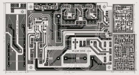
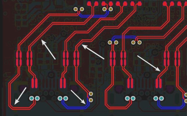
1. Pad Overlap: Pad overlap occurs when holes overlap during the drilling process, leading to damage and scrapping. To avoid this, ensure proper spacing between pads to prevent overlapping during drilling.
2. Graphics Layer Misuse: Avoid unnecessary connections on graphics layers to prevent confusion. Design boards with the appropriate number of layers for clarity and adherence to conventional design practices. For example, place component surface designs on the top layer and solder surface designs on the bottom layer to facilitate assembly.
3. Random Characters: Avoid placing SMD solder pads over characters, as this complicates testing and component soldering. Ensure characters are appropriately sized for clear screen printing without overlapping, balancing legibility with space constraints.
4. Single-Sided Pad Aperture Setting: For single-sided pads that aren’t drilled, set the hole diameter to zero to prevent issues during drilling data generation. Designing numerical values may cause coordinate problems during manufacturing.
5. Use of Filler Blocks for Pad Drawing: While filler blocks may pass DRC inspections, they can hinder processing. During solder resist application, filler block areas may be covered, making device soldering difficult. Avoid using filler blocks for pads to ensure smooth processing.
As a professional FPC soft board manufacturer, WellCircuits Limited is honored to have collaborated with many clients. We are committed to assisting our new customers in any way possible. Please don’t hesitate to reach out if you have any questions or need assistance.


