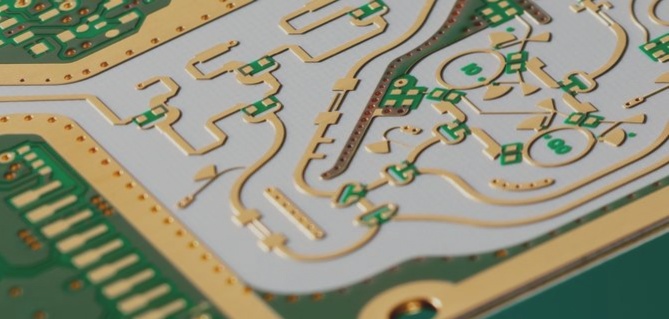
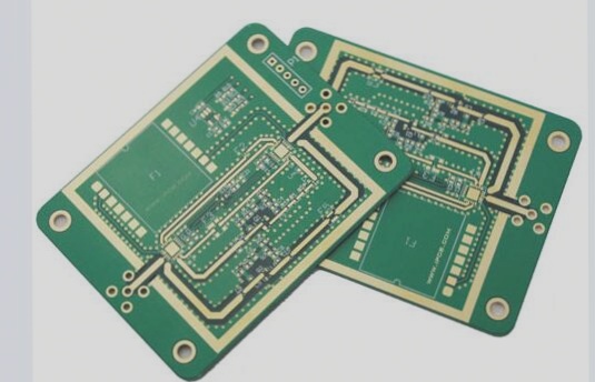
PCB Component Layout Best Practices
1. Basic Rules of PCB board Component Layout
- Consider circuit modules with components of the same function densely concentrated.
- Separate digital and analog circuits.
- Avoid mounting components near non-mounting holes and mounting holes.
- Avoid vias below horizontally mounted components.
- Maintain a 5mm distance between outer components and the board edge.
- Keep a 2mm distance between the outer pad of a mounted component and adjacent components.
- Avoid contact between metal shell components and other parts.
- Distribute heating elements evenly and keep them away from wires.
- Arrange power sockets around the printed board.
- Align IC components on one side with clear polarity markings.
- Ensure proper wiring density on the board.
- Avoid through-holes on patch pads.
- Ensure consistency in patch alignment and polarity marking.
2. Component Wiring Guidelines
- Avoid wiring within 1mm of the PCB edge and around mounting holes.
- Maintain specific widths for power and signal lines.
- Ensure proper dimensions for via holes and component pads.
- Radial arrangement for power and ground wires.
- Avoid looping signal wires.
3. Enhancing Anti-Interference and EMC
Strategies to improve anti-interference and electromagnetic compatibility in electronic product development:
- Pay attention to systems with high clock frequencies and fast bus cycles.
- Address systems with high-power drive circuits.
- Focus on systems with weak analog signal circuits.
Tips for reducing noise and interference:
- Opt for low-speed chips when possible.
- Use resistors in series to reduce edge transition rates.
- Provide damping for components like relays.
- Utilize clock generators meeting system requirements.
- Keep clock wires short and ground clock areas.

The Best Practices for PCB Layout
- Place the I/O drive circuit close to the edge of the printed board to minimize signal travel time.
- Filter incoming signals and those from high-noise areas to improve signal quality.
- Utilize serial terminal resistance to reduce signal reflection.
- Connect unused ends of MCD to high, ground, or define as output.
- Ensure integrated circuit ends meant for power supply ground are connected.
- Avoid leaving input terminals of unused gate circuits floating.
- Ground the positive input terminal of unused operational amplifiers and connect the negative input terminal to the output terminal.
- Prefer 45-fold lines over 90-fold lines on printed boards to reduce external emission and signal coupling.
- Divide the printed board based on frequency and current switching characteristics.
- Use single-point power supply and grounding for boards, ensuring thick power and ground lines.
- Keep clock, bus, and chip select signals away from I/O lines and connectors.
- Separate analog voltage input and reference voltage terminals from digital circuit signal lines.
- Unify digital and analog parts for A/D devices rather than crossing them.
- Ensure clock lines are perpendicular to I/O lines to minimize interference.
- Keep component pins and decoupling capacitor pins as short as possible.
- Use thick lines for key signals and add protective ground on both sides.
- Avoid routing wires under quartz crystals and noise-sensitive devices.
- Avoid forming current loops around low-frequency circuits in weak signal circuits.
- Minimize loop areas for any signal routing.
- Include one decoupling capacitor per IC and add high-frequency bypass capacitors near electrolytic capacitors.
- Opt for tantalum or polycooled capacitors over electrolytic ones for circuit charge and discharge energy storage.
- Ground the case of tubular capacitors on the PCB board.