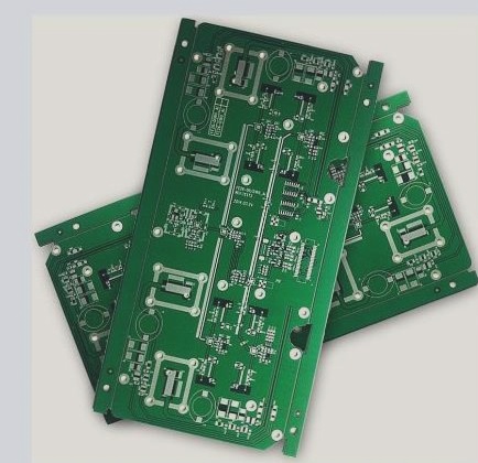
Essential PCB Layout Tips for Designing a Reliable Circuit Board
- Ensure proper spacing between traces to avoid short circuits during manufacturing.
- Achieve copper balance on both sides of the PCB for optimal performance.
- Minimize EMI by using closely spaced solid planar return paths for signal traces.

- Avoid 90-degree trace angles; opt for 45-degree angles for improved reliability.
- Widen power and ground traces to enhance current flow and reduce heat buildup.
- Utilize vias for heat dissipation and electrical connections between layers.
- Enhance EMI shielding and heat dissipation by using a solid copper layer for the power layer.
- Place the reference point on the same side as SMT components for accurate assembly.
- Use power planes to distribute power effectively across the PCB.
- Consider buried vias in dense designs for efficient use of space.
- Assign unique drill size symbols for different hole types to maintain clarity in design.
- Create a symmetrical stack by alternating signal and plane layers around the PCB centerline.
- Choose trace width that suits your manufacturer’s capabilities.
- Route critical signals along the shortest path with minimal vias.
- Connect test points to power and ground networks for easier testing.
- Avoid placing test points near tall components to simplify evaluation.
- Leave ample space between traces and mounting holes to prevent hazards.
- Adjust trace width proportionally to trace height to avoid erosion during manufacturing.

