Typesetting Engineering Overview
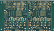
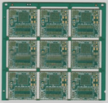
After verifying your PCB layout, it undergoes conversion into production data. This data is then integrated into a standard panel with other layouts to facilitate seamless production, a process commonly known as “typesetting.”

Key Considerations for Typesetting:
- Layout data sharing the same solder mask, copper thickness, and surface finish are typically grouped together in a standard panel.
- Occasionally, HASL (Hot Air Solder Leveling) PCBs may be included in a standard panel with an ENIG (Electroless Nickel Immersion Gold) finish. Customers have the option to reject this upgrade by selecting the appropriate button on the order page.
- For multi-layer PCBs, inner layer production data with a smaller copper thickness may be combined in a standard panel that typically uses a larger copper thickness. If your design requires a specific copper thickness for impedance control or other reasons, you can specify this during the ordering process or communicate it to your sales representative. You also have the option to decline the default setting.


If you have any inquiries regarding PCBs and PCBA, please reach out to us at info@wellcircuits.com.