The Evolution of HDI Technology in PCB Manufacturing
With the demand for thinner and more compact electronic devices, High-Density Interconnect (HDI) technology has emerged as a key player in the production of ultra-thin and high-density PCBs. These advanced boards boast smaller sizes, increased hole density, and intricate trace layouts, resembling a carrier board.
Latest Updates on Ultra-Thin and High-Density Blind Hole Products:
Manufacturing ultra-thin, high-density HDI multi-layer boards involves a complex process that includes laminated pressing using FR4 resin, semi-cured sheets, and electrolytic copper foil. Challenges such as lamination of thin core plates, mechanical and laser drilling, and core plate expansion management are key focus areas during production.
Product Details and Lamination Design:
- Four-layer first-order HDI (1 + 2 + 1)
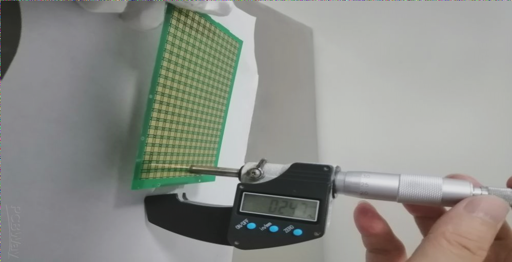
- Board thickness: 0.25mm ± 0.025mm
- Minimum mechanical hole size: 0.1mm with 282,038 holes
- Minimum laser hole size: 0.1mm with 1,345,698 holes (both sides)
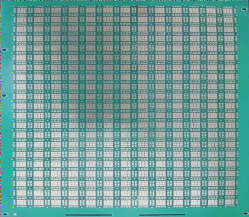
- Individual size: 5 * 5mm, 546 pieces per set
Key Control Points in Production:
- Internal Drilling: Utilizing custom drilling tools for 282,038 holes with a core plate thickness of 0.065mm. Careful handling to prevent plate deformation is crucial.
- Lamination Pressure: Maintaining precise pressure and glue distribution during the 0.22mm pressing process is critical for achieving desired laminate thickness.
- Laser Drilling: Managing high-density laser holes with controlled energy levels to ensure quality and prevent breakdowns.
- Electroplated Plug Holes and Surface Copper: Filling laser holes with a baffle due to the thin plate and copper layer requirements.
- Soldermask: Applying soldermask with Laser Direct Imaging for small pads and utilizing a nickel-palladium-gold surface treatment process.
Product Showcase:
Visual representation of product layers, final thickness, and appearance:
- Product Layer Thickness:

- Final Plate Thickness:

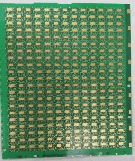
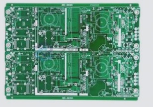
- Finished Product Appearance:

For inquiries about PCBs or PCBA, reach out to us at info@wellcircuits.com

 العربية
 简体中文
简体中文 Nederlands
 English
 Français
 Deutsch
 Italiano
 日本語
日本語 한국어
한국어 Português
 Русский
 Español
 ไทย
ไทย