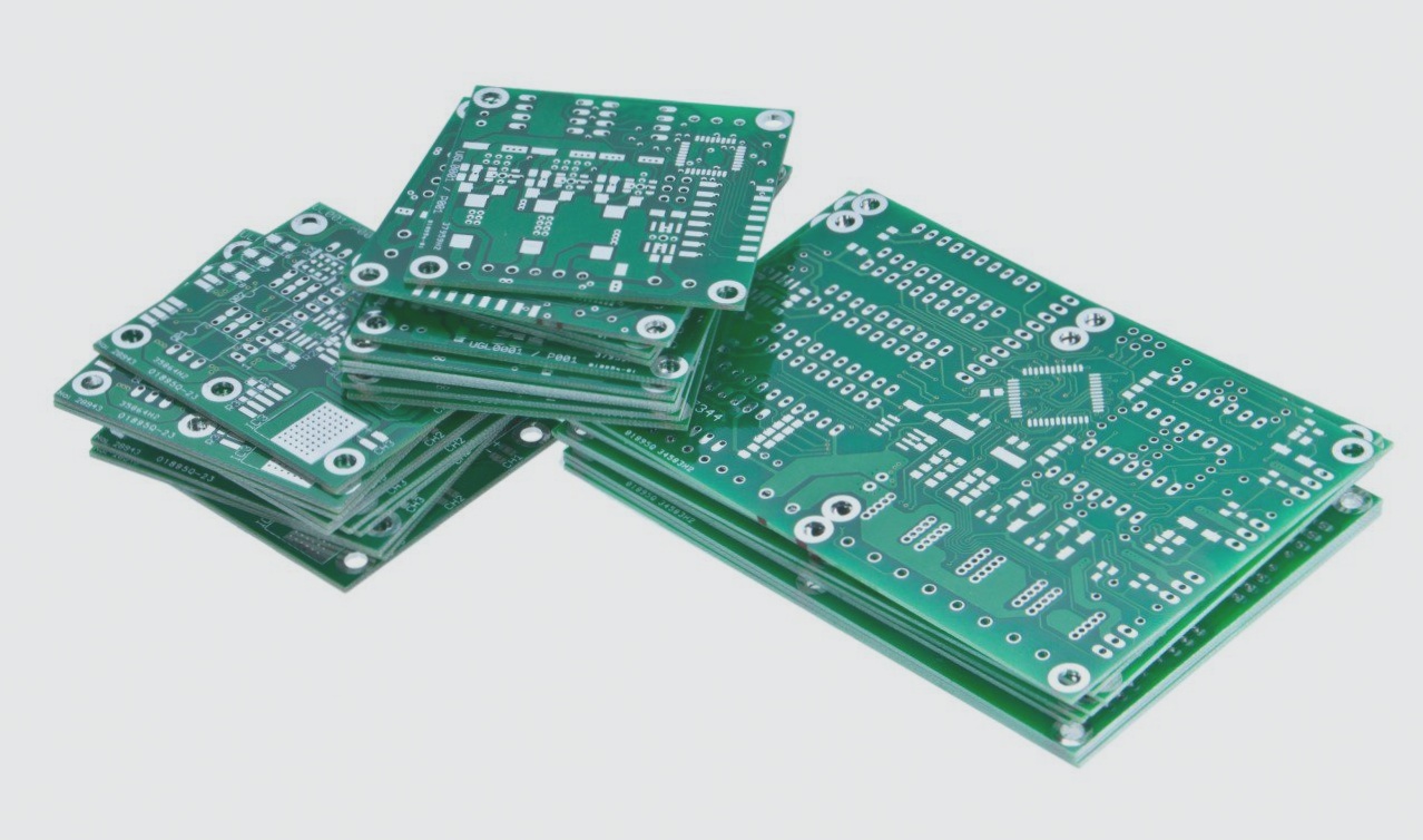
Various production techniques and material sets are employed for FPCs, with a notable distinction being the dimensional properties. Rigid printed circuits typically boast greater dimensional stability compared to the commonly used polyimide film, which serves as the foundation in 98% of flex circuits manufactured. This increased dimensional variability necessitates different design considerations for flexible circuits in contrast to their rigid PCB counterparts. Unfortunately, much of the available design software relies on rigid PCB layout guidelines, leading to potential manufacturing and operational issues for flexible circuits. Preparing a flexible circuit design for fabrication is often referred to in the industry as “flexizing” the layout.
The following outlines five common methods through which “flexizing” enhances a design’s durability, manufacturability, and readiness for construction.

Spacing between solder pads as well as surrounding traces: Here lies the tradeoff, a design compromise based on factor #1. When the cover film or solder mask openings are enlarged, the edges of the surrounding conductor traces may be exposed if they are positioned too closely to a solder pad. This can lead to shorts if solder bridges form between port pins or pads. The physical dimensions of the circuit are another factor that can affect registration ability. Generally, more space is required between a solder pad and a nearby conductive trace to accommodate the cover film or solder mask without encountering resistance.
Stress points in conductors: Since flex wiring is utilized in both fold-to-mount and dynamic bending applications, trace configurations that are suitable in a rigid PCB might pose issues in a flexible circuit. Conductor traces with sharp corners and acute points at the base of solder pads become natural “stress points” when the area near them is flexed. This can result in trace fractures or delamination. A well-designed flexible circuit will have a smooth curvature for conductor turn points (rather than sharp edges) and a gentle radius from the trace to the pad fillet instead of a sharp angle. Selective attachment of stiffeners will prevent bending in rigid areas and is a common design practice.
Stacked traces: Traces on opposite sides of the dielectric should not directly “stack” on each other. Traces under tension (on the outside of the bend radius) may fracture when the circuit is bent if they directly align in parallel with a trace on the opposite side. The traces under tension are forced farther from the neutral axis of the folded region and can crack, especially with repeated bending. A good design practice is to keep the copper in the neutral axis of a bend by intentionally designing this area as a single conductive layer. When this is not feasible, a proper design will “stagger” the traces between top and bottom copper layers to prevent top and bottom alignment.
Solder joints too close to flex point: A solder joint is formed by an intermetallic bond of the solder alloy to the copper trace. While the copper trace is typically flexible, areas that have been soldered become very rigid and inflexible. When the substrate is bent near the edge of the solder joint, the solder pad is either going to crack or peel. Either scenario will cause significant functional issues. The bottom line is that creating a flex circuit with conventional PCB software can lead to serious manufacturability and reliability issues. It is best to collaborate with your flexible circuit vendor or a flexible circuit design expert to either “flexibilize” the design before commencing manufacture or to design the layout directly from a web list. This will ensure that the design can be manufactured to meet your requirements.

