With the continuous advancements in the electronics industry, multi-layer circuit boards are increasingly preferred. For high-frequency multi-layer boards, all VIA holes under the BGA must be properly handled. The solder mask should be double-sided with defined points, avoiding plug holes. Typically, PCB plug holes are placed beneath the ground solder mask layer, followed by a second layer of ink to fill heat dissipation holes smaller than 0.5mm.
(1) During DIP soldering of components, care must be taken to prevent solder from penetrating and causing short circuits.
(2) Ensure the PCB surface remains flat to meet the required characteristic impedance and customer specifications.
(3) Prevent damage to circuit lines.
WellCircuits Limited offers two types of plugging services tailored to customer needs: “resin plugging” and “electroplating filling”. Resin plugging involves using solvent-free ink to address issues of difficult filling and reduces the risk of ink cracking during heating.
Electroplating hole filling utilizes additives to control the copper deposition rate, particularly useful for continuous multi-layer laminated hole boards or high-current PCB designs.
(1) Avoid flux residue in the via, which can cause blockage;
(2) Prevent solder beads from popping out during wave soldering to avoid line short circuits;
(3) Prevent surface tin from flowing into the holes, causing solder bridges that affect final assembly quality;
(4) After surface mounting components are completed, the PCB board needs to undergo testing using a testing machine. Only those where vacuum suction forms a negative pressure are considered qualified.
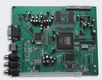
Before understanding PCB solder mask openings, let’s first define the solder mask layer! The PCB solder mask layer refers to the part of the printed circuit board coated with green protective ink. The PCB solder mask opening refers to the areas where the copper pads must be exposed, allowing solder to protrude through the board.
For double-sided circuit boards, both sides are coated with a solder mask to prevent oxidation and facilitate subsequent SMT soldering. PCB solder mask opening ensures that copper around apertures remains exposed; covering it with ink would prevent signal measurement and surface leakage, potentially affecting trace thickness and current capacity.
1: Liquid photosensitive ink: Liquid photosensitive ink is a special type of ink that can be directly printed onto a substrate without the need for a printing plate. The ink coating undergoes curing upon exposure to light and, after development, can undergo processes such as etching, electroplating, electrophoresis, and coloring. This makes it suitable for producing small batches, multiple varieties, and high-precision products with personalized designs.
2: UV solder mask ink: This ink is designed for manufacturing solder mask patterns on rigid printed circuit boards. It features rapid light fixation, excellent heat resistance, and strong adhesion, meeting the requirements for both single-sided and double-sided circuit boards. If the viscosity is too high, a small amount of special diluent can be added for dilution, but the quantity should not exceed 5% of the total ink volume.
当然,请提供文章内容,我将帮助您进行修改和润色。
(1) During DIP soldering of components, care must be taken to prevent solder from penetrating and causing short circuits.
(2) Ensure the PCB surface remains flat to meet the required characteristic impedance and customer specifications.
(3) Prevent damage to circuit lines.
WellCircuits Limited offers two types of plugging services tailored to customer needs: “resin plugging” and “electroplating filling”. Resin plugging involves using solvent-free ink to address issues of difficult filling and reduces the risk of ink cracking during heating.
Electroplating hole filling utilizes additives to control the copper deposition rate, particularly useful for continuous multi-layer laminated hole boards or high-current PCB designs.
(1) Avoid flux residue in the via, which can cause blockage;
(2) Prevent solder beads from popping out during wave soldering to avoid line short circuits;
(3) Prevent surface tin from flowing into the holes, causing solder bridges that affect final assembly quality;
(4) After surface mounting components are completed, the PCB board needs to undergo testing using a testing machine. Only those where vacuum suction forms a negative pressure are considered qualified.
Before understanding PCB solder mask openings, let’s first define the solder mask layer! The PCB solder mask layer refers to the part of the printed circuit board coated with green protective ink. The PCB solder mask opening refers to the areas where the copper pads must be exposed, allowing solder to protrude through the board.
For double-sided circuit boards, both sides are coated with a solder mask to prevent oxidation and facilitate subsequent SMT soldering. PCB solder mask opening ensures that copper around apertures remains exposed; covering it with ink would prevent signal measurement and surface leakage, potentially affecting trace thickness and current capacity.
1: Liquid photosensitive ink: Liquid photosensitive ink is a special type of ink that can be directly printed onto a substrate without the need for a printing plate. The ink coating undergoes curing upon exposure to light and, after development, can undergo processes such as etching, electroplating, electrophoresis, and coloring. This makes it suitable for producing small batches, multiple varieties, and high-precision products with personalized designs.
2: UV solder mask ink: This ink is designed for manufacturing solder mask patterns on rigid printed circuit boards. It features rapid light fixation, excellent heat resistance, and strong adhesion, meeting the requirements for both single-sided and double-sided circuit boards. If the viscosity is too high, a small amount of special diluent can be added for dilution, but the quantity should not exceed 5% of the total ink volume.
当然,请提供文章内容,我将帮助您进行修改和润色。