Common PCB Surface Treatment Processes
- Tin Spraying (Lead-Free or Leaded)
- Hot Air Leveling (HAL)
- Organic Coating
- Chemical Gold Plating
- Electroplating Nickel Gold
- Immersion Silver
- Immersion Tin
- Carbon Oil
- Halogen-Free Gold Finger
- OSP for Anti-Oxidation
As environmental protection becomes a top priority in PCB production, the use of leaded tin spraying processes is decreasing. Many companies are now turning to lead-free tin spraying methods to adhere to ROHS environmental standards. Non-compliance with these standards can hinder passing basic audits and establishing long-term product development partnerships.
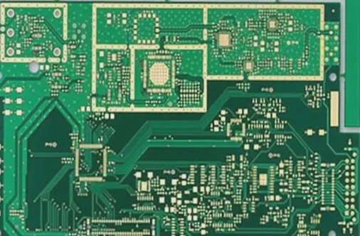
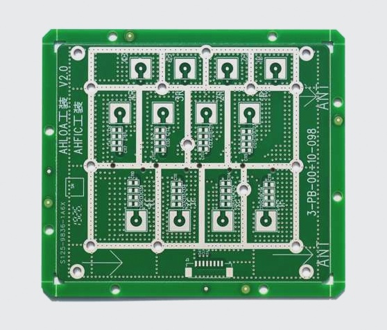
The surface treatment technology for printed circuit boards involves applying layers to PCB components and electrical connection points to enhance their mechanical, physical, and chemical properties from the base material. This is crucial for ensuring good solderability and electrical properties, as direct copper exposure can lead to oxidation. Hence, surface treatment processes play a vital role in PCB production across various industries.
Definition of Each PCB Surface Treatment Process
1. Tin Spraying (Hot Air Leveling)
The tin spraying process involves coating the PCB surface with molten tin and lead solder, which is then leveled using heated compressed air. This creates a protective layer against copper oxidation, ensuring good solderability. The process includes micro-etching, preheating, flux application, tin spraying, and cleaning.
2. OSP (Organic Solderability Preservatives)
OSP forms a barrier layer between copper and the environment by chemically growing an organic film on a clean copper surface. This film provides excellent oxidation, thermal shock, and moisture resistance, protecting the copper from environmental damage. The process involves degreasing, micro-etching, pickling, pure water cleaning, organic coating, and final cleaning.
3. Chemical Gold Plating (Electroless Nickel Plating/Immersion Gold)
Chemical gold plating applies a thick layer of gold onto the copper surface of PCBs, enhancing electrical properties and extending protection. The process involves the diffusion of electroless nickel coating between the gold and copper layers, preventing direct diffusion and ensuring PCB integrity. This plating method inhibits copper dissolution, making it ideal for lead-free soldering applications.
Chemical Gold Manufacturing Process
- Depickling and cleaning
- Micro-etching
- Pre-preg treatment
- Activation
- Electroless nickel plating
- Chemical immersion gold
The chemical gold manufacturing process involves six chemical tanks and approximately 100 different chemicals, making it a relatively complex procedure.
Immersion Silver Process
The immersion silver PCB processing provides simplicity and speed, eliminating the need for a thick PCB armor layer. It ensures good electrical properties and robust solderability under various environmental exposures. However, tarnishing may occur due to the absence of a nickel layer beneath the silver coating.
The silver immersion process includes a displacement reaction that deposits a sub-micron layer of pure silver. Organic compounds are incorporated to prevent silver corrosion and mitigate migration issues.
Tin Immersion Process
Tin immersion processes for PCB surface treatment utilize tin-based solders compatible with various solder types. Organic additives have been introduced to address tin whisker formation, enhancing thermal stability and solderability.
Electroplating Nickel Gold Process
Electroplating nickel gold involves applying a layer of nickel followed by a layer of gold on the PCB surface. This process prevents diffusion between gold and copper, with variations like “soft gold” and “hard gold plating” offering different applications.
Electroless Palladium Plating Process
Electroless palladium plating, similar to electroless nickel plating, provides excellent welding reliability, thermal stability, and surface flatness. However, the rarity of palladium contributes to increased production costs.