A 6-layer PCB board consists of six layers of conductive material. Typically, it includes four signal layers and two planes (one for power supply and one for grounding) sandwiched between the signal layers. This design significantly reduces electromagnetic interference, facilitates optimal routing for both low-speed and high-speed signals, and enhances the transmission efficiency of signals.
When compared to a double-layer surface, a 6-layer PCB provides superior capabilities for achieving desired line layouts, especially necessary for products with compact dimensions and stringent requirements. If a double-sided panel fails to meet customer expectations in terms of line layout effectiveness, upgrading to a 6-layer PCB becomes essential.
Optimizing the stack-up configuration of a 6-layer PCB can further enhance its overall performance, especially in RF applications where precise control over electromagnetic interference is critical. Proper design must also incorporate multiple isolation components to mitigate any potential errors that could compromise the PCB’s performance.
In conclusion, when designing a 6-layer PCB board, meticulous attention to the stack-up and component placement is imperative to fully harness its capabilities and ensure optimal performance across various applications.

—
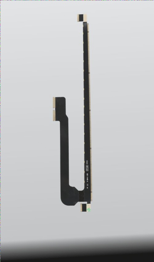
Image 1: Rigid-flex 6-layer PCB HDI
The number of ground, power, and signal layers required for the PCB should be carefully analyzed and determined prior to designing a 6-layer PCB board. The adhesive layer plays a crucial role in the laminate, enhancing shielding effectiveness and reducing the need for external shielding. When designing dense circuit boards with limited wiring space, a typical configuration includes four signal layers, one ground plane, and one power plane. In high-density circuit boards, wireless and analog signals are integrated.
The layer stackup of signal/ground/power/signal/ground/signal plane facilitates separation between internal and external signal layers. This layered approach aids in mitigating electromagnetic interference within internal signal layers and is particularly beneficial for RF equipment, providing AC power decoupling and grounding.
For constructing printed circuit boards with sensitive circuits, a stackup such as signal/power/2x signal/ground/signal is often chosen to effectively safeguard sensitive wiring. This configuration is well-suited for high-frequency analog signals or high-speed digital circuits.
These signals are separated from low-speed signals on the outer layers, with shielding provided on the inner layers, allowing for signal routing at varying frequencies and switching speeds. A stackup like ground/signal/power/ground/signal/ground can be strategically placed near strong radiation sources on the circuit board to manage electromagnetic interference effectively, making it suitable for boards used in noisy environments.
—
This revision aims to clarify and streamline the technical details while ensuring the information remains clear and coherent.

Image 2: 6 layer flexible PCB example
The primary principle of layout design focuses on effective partitioning, specifically segregating analog and digital devices to minimize interference. Digital signals tend to generate substantial interference but also possess strong immunity against it, whereas analog signals generate less interference but are more vulnerable to digital signal noise. Additionally, careful attention must be given to segregating components with different operating voltages, ensuring devices with significant voltage discrepancies are spaced sufficiently apart.
For decoupling capacitors associated with chips, proximity to the pins is crucial for optimal performance. Furthermore, pins belonging to the same network should be grouped closely together, while maintaining a visually appealing layout. The segmentation process can be detailed as follows:
A. Highlight a specific voltage network, transition to the inner power layer, use lines to delineate a closed contour, defining the boundaries of the voltage network.
B. Route the top layer and ground layer pins using traces, connecting them to the inner power layer via pads.
C. Define subsequent power networks with clear lines marking the boundary between the two networks, ensuring clarity and precision in layout execution.

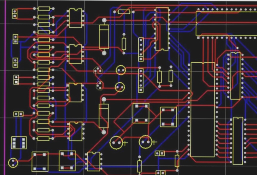
Image 3: Component Layout
Attention should be paid to the internal electrical layers: ensure adequate spacing for areas with significant voltage differences. Unused copper areas can be placed on planes to facilitate their controlled corrosion. Avoid placing pads on split lines to ensure proper contact with the internal electrical layers.
—
I adjusted the wording slightly to improve clarity and correctness.


