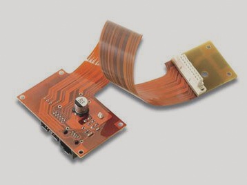
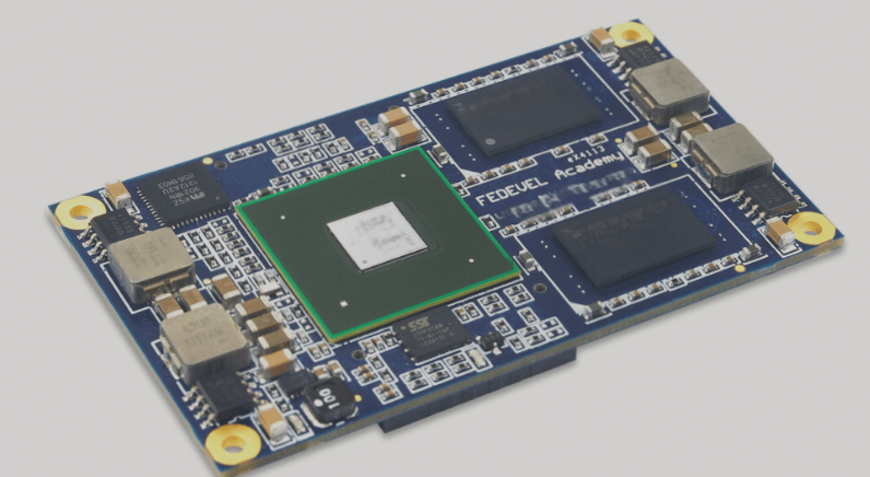
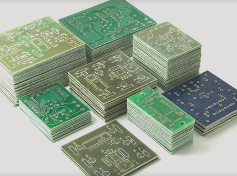
This article introduces 7 ways to quickly judge the quality of PCB design. The focus here is on layout and component placement, not the actual quality of the circuit board structure itself (it all depends on the circuit board manufacturer).
Finally, this article is not intended to be highly technical, and certainly will not cover all possibilities, especially for highly complex designs or designs with unique requirements. The purpose of this article is to show you how to quickly determine whether you have a bad PCB design because there are some specific areas in PCB design, and new designers are most likely to do these things wrong.
1-Circuit board routing
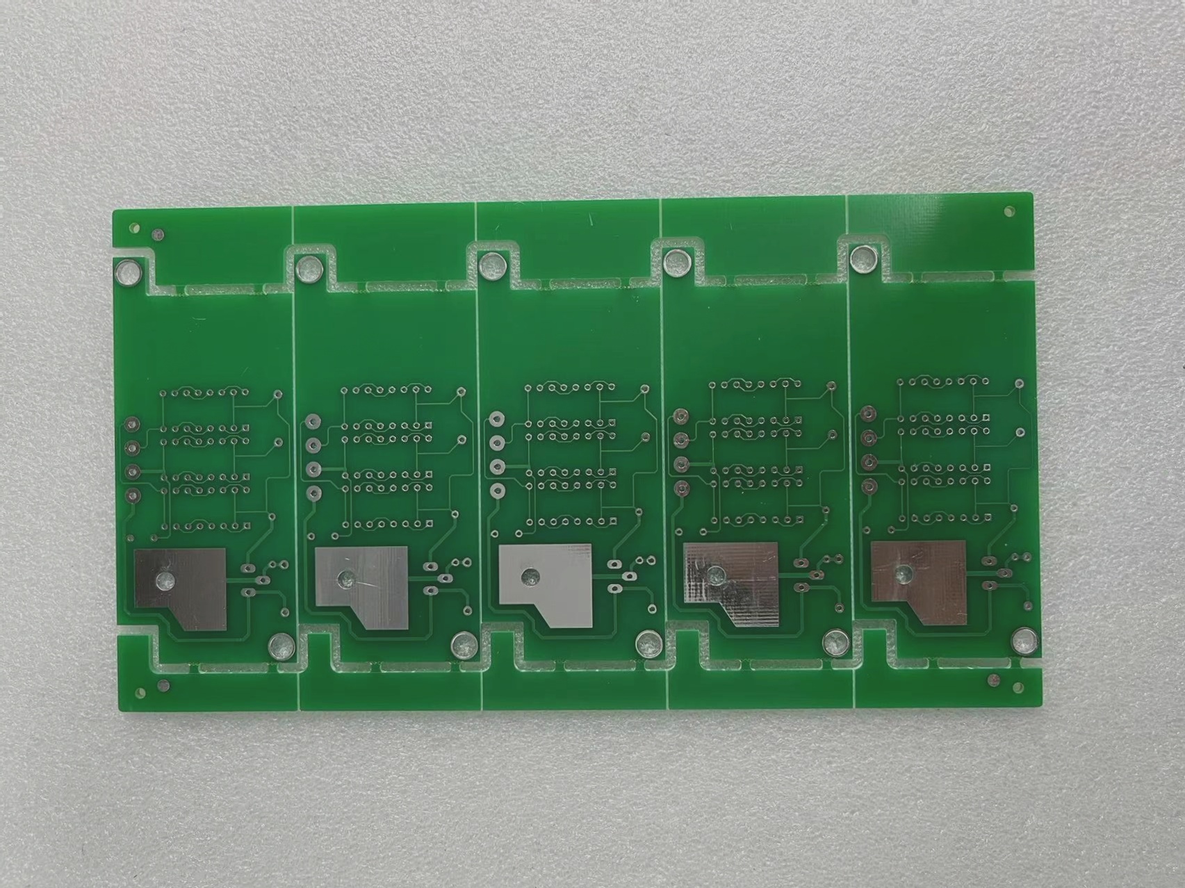
Take a look at the visible traces on the circuit board in general. These will be covered by solder resist, which is a thin layer of lacquer-like polymer, covering the copper traces to prevent oxidation and short circuits. This layer is usually green, but other colors can also be used. Please note that the white solder mask tends to make the traces the hardest to see. In most cases, just use standard green. In addition, only the top and bottom layers are actually visible, and if the board has more than two layers, you will not see the inner layers. Nevertheless, reviewing only the external layer should still provide some clues about the quality of the design.
First, check to see if all traces extend in straight segments without sharp bends. Sharp angles may cause trouble for certain high-power and high-frequency traces. Rather than trying to determine which traces can be bent 90 degrees, it is better to avoid them. In any case, most CAD PCB layout software packages can be set up to avoid this problem. Please note that there are some exceptions. Some printed inductors are square concentric spirals, and some printed antennas have sharp bends. However, both of these are easy to identify.