Electromagnetic Compatibility (EMC) and Electromagnetic Interference (EMI) in PCB Design
Electromagnetic Compatibility (EMC) and Electromagnetic Interference (EMI) are critical considerations for PCB design engineers, especially with the increasing complexity of modern PCB layouts and the demand for high-speed systems from OEMs. EMC involves the generation, transmission, and reception of electromagnetic energy, which must be carefully managed to prevent interference in PCB designs. EMI, a negative outcome of EMC, can disrupt the functionality of electronic systems if not properly addressed.

7 Tips to Mitigate Electromagnetic Issues in PCB Design:
- Tip 1: Grounding Strategy
- Tip 2: Segregate Analog and Digital Circuits
- Tip 3: Address Crosstalk and Trace Layout
Effective grounding is key to reducing EMI. Design the PCB ground plane meticulously to minimize emissions, crosstalk, and noise. Ensure each component connects to a reliable ground point for optimal neutralization. Utilize multiple stable voltages with corresponding ground planes strategically to balance cost and EMI reduction.
Segregate analog and digital circuits to prevent interference. Keep high-amperage analog circuits separate from high-speed digital traces. Implement low-pass filters to eliminate high-frequency noise and maintain signal stability. Separate ground planes for analog and digital signals to preserve signal integrity.
Importance of Traces in PCB Design
Traces play a crucial role in ensuring proper current flow in PCBs. It is essential to manage current flow effectively to prevent issues such as electromagnetic interference (EMI) and electromagnetic compatibility (EMC).
Separation of Current and Ground
When dealing with high-speed signals from devices like oscillators, it is vital to separate the current from the ground plane. Running current in parallel with another trace can lead to problems such as crosstalk, where signals interfere with each other.
Decoupling Capacitors
Decoupling capacitors are essential components that help reduce crosstalk and noise. Placing them between power and ground pins can ensure low AC impedance, improving signal quality over a wide frequency range.
Avoiding 90-Degree Angles
To minimize EMI, it is recommended to avoid using traces, vias, or components with 90-degree angles. Right angles can increase capacitance, change impedance, and cause reflections, leading to electromagnetic interference.
Caution with Vias
While vias are necessary for connecting different layers in PCBs, they can introduce inductance and capacitance. Careful placement and usage of vias are crucial to avoid signal delays, impedance changes, and reflections in the traces.
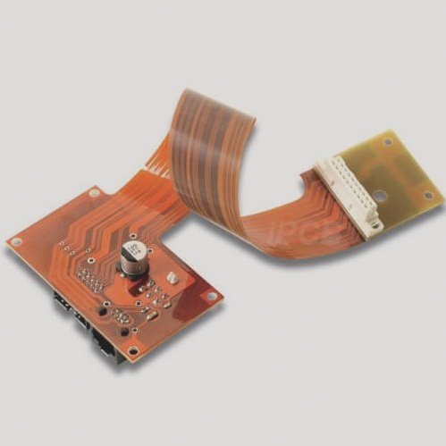
Cables and Shielding
Cables carrying digital or analog signals can create parasitic capacitance and inductance, contributing to EMC issues. Using shielded cables and physical shielding can help reduce EMI interference and improve overall signal integrity.