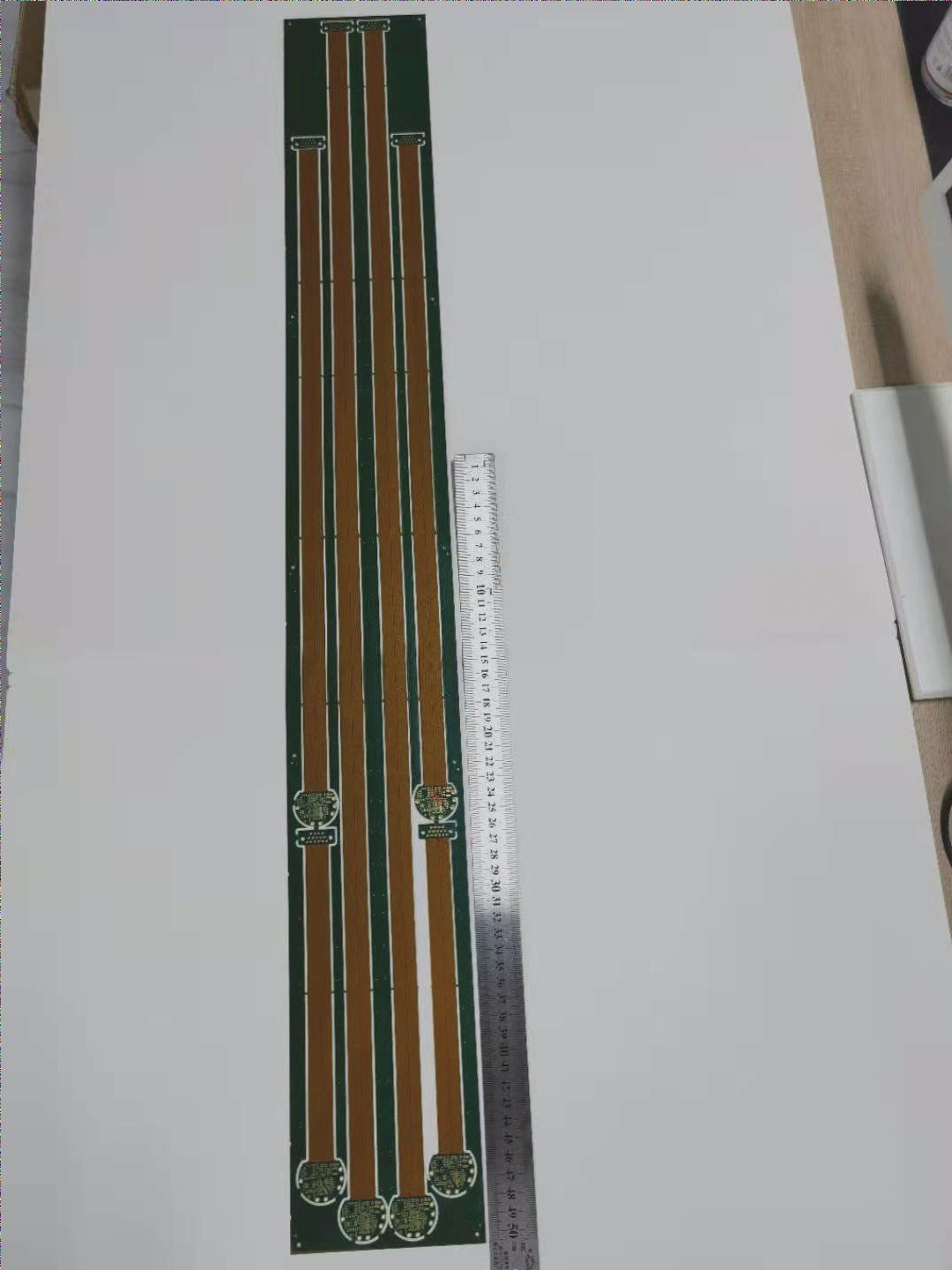
The basic design process of a general PCB board is as follows:
1. **Preliminary Preparation**
This includes preparing component libraries and schematics. To do a good job, you must first sharpen your tools.” To create a quality PCB board, you need to focus not only on the design principles but also on drawing accurately. Before starting the PCB board design, prepare both the schematic (SCH) component library and the PCB component library. You can use the libraries provided by Protel, but these may not always meet your needs. It is often better to create a component library yourself based on the standard size data of the selected devices. Ideally, create the PCB component library first, then the SCH component library. The PCB component library has stringent requirements as it directly impacts the board’s assembly. The SCH component library requirements are more relaxed; ensure that pin attributes and relationships with PCB components are well-defined. Note: Pay attention to hidden pins in the standard library. Once this is complete, you can proceed with designing the schematic diagram, and once finished, start the PCB board design.
2. **PCB Board Structure Design**
At this step, draw the PCB board surface in the PCB design environment based on the determined circuit board size and mechanical positioning. Place connectors, buttons/switches, screw holes, assembly holes, etc., according to the positioning requirements. Carefully determine the wiring and non-wiring areas (e.g., the area around screw holes should be designated as non-wiring).
3. **PCB Board Layout**
Layout involves placing devices on the board. If the preparations mentioned above are complete, generate a netlist (Design-Create Netlist) from the schematic and then import it (Design-Load Nets) into the PCB board design. Initially, you might see devices piled together with flying wires between pins indicating connections. Place the devices according to the following principles:
1) **Functional Division**: Separate digital circuit areas (prone to interference), analog circuit areas (sensitive to interference), and power drive areas (sources of interference).
2) **Component Placement**: Place components that perform the same function close together to simplify connections. Adjust the relative positions of functional blocks to minimize connection complexity.
3) **Consider Mass and Heat**: For large components, consider the installation position and strength. Place heating elements separately from temperature-sensitive components, and consider thermal convection if needed.
4) **I/O Drive Devices**: Place these close to the edge of the printed board and the lead-out connector.
5) **Clock Generators**: Position clock generators (e.g., crystal oscillators) close to the devices that use the clock.
6) **Decoupling Capacitors**: Add a decoupling capacitor (usually a monolithic capacitor with good high-frequency performance) between each integrated circuit’s power input pin and ground. For densely populated boards, consider adding tantalum capacitors around several integrated circuits.
7) **Discharge Diodes**: Include a discharge diode for the relay coil (e.g., 1N4148).
8) **Layout Balance**: Ensure the layout is balanced, dense, and orderly. Avoid top-heavy or heavy areas. When placing components, consider their actual size (occupied area and height) and their relative positions. Modify placement as needed to reflect the principles mentioned while maintaining neatness and aesthetic appeal. This step affects the overall appearance of the board and the difficulty of wiring in the next step, so thorough consideration is necessary. Preliminary wiring can be done in uncertain areas.
4. **Wiring**
Wiring is a critical process in PCB board design and directly impacts performance. There are generally three aspects of wiring:
1) **Layout Wiring**: This is the basic requirement for PCB design. An unorganized board with flying wires is unacceptable.
2) **Electrical Performance**: After routing, adjust the wiring to achieve optimal electrical performance.
3) **Aesthetics**: Well-organized wiring not only affects the board’s appearance but also facilitates testing and maintenance. Ensure wiring is neat and uniform, avoiding criss-crossing or disorderly patterns. The wiring must ensure the performance of the electrical appliance while meeting individual requirements, otherwise, it may be discarded. Wiring should follow these principles:
1) **Power and Ground Lines**: Wire these first to ensure circuit board performance. Widen power and ground wires where possible, with the general order being: ground wire > power wire > signal wire. Signal wire width typically ranges from 0.2-0.3mm, with thin wires down to 0.05-0.07mm, and power cords generally range from 1.2-2.5mm. For digital circuits, use a wide ground wire to form a loop; avoid this for analog circuits.
2) **High-Frequency Lines**: Route lines with strict requirements (e.g., high-frequency lines) first, and avoid adjacent parallel lines between input and output to prevent reflection interference. Use ground wire isolation if necessary, and ensure adjacent layer wiring is perpendicular to minimize parasitic coupling.
3) **Oscillator and Clock Lines**: Ground the oscillator shell, keep the clock line as short as possible, and avoid spreading it across the board. Increase ground area below high-speed logic circuits, and avoid using signal lines to minimize surrounding electric fields.
4) **Line Bends**: Use 45-degree bends instead of 90-degree angles to reduce high-frequency signal radiation; double arcs are preferable for high-precision lines.
5) **Avoid Loops**: Do not form loops in signal lines; if unavoidable, keep them as small as possible. Minimize vias in signal lines.
6) **Key Lines**: Keep key lines short and thick, adding protective ground on both sides.
7) **Sensitive Signals**: For sensitive signals and noise fields transmitted through flat cables, use the “ground-signal-ground” method.
8) **Test Points**: Reserve test points for key signals to facilitate production and maintenance.
9) **Optimization**: After completing schematic wiring, optimize the layout. Perform network and DRC inspections, and fill unwired areas with ground wires. Use large copper areas for ground or consider a multi-layer PCB with separate layers for power, ground, and signal.


