Introduction to Non-Isolated DC-to-DC Buck Converters
DC-to-DC buck converters play a crucial role in electronics, with the Buck converter being the most commonly used type among Buck, Boost, and Buck-Boost converters. A new compact buck converter board is introduced in this post, supporting input voltages from 8V to 95V and delivering a stable 5V at 1A output.
Controller Chip and Circuit Stability
The circuit utilizes the MP9486 controller chip, known for its high frequency and sensitivity. Despite initial reports of instability, modifications have been made to ensure reliable operation within the specified voltage range and output current handling capacity.
Design Tools and Component Sourcing
Altium Designer 23 was used for schematic and PCB design, with collaboration facilitated through Altium 365. The Octopart component search engine aided in sourcing components and generating the Bill of Materials (BOM). Gerber files were submitted to Wellcircuits for high-quality board fabrication.
Testing and Validation
Rigorous testing was conducted under various conditions using specialized equipment like the Siglent SDL1020X-E DC load, SDM3045M multimeter, and SDS2102X Plus oscilloscope. The circuit has been proven to meet the requirements for a high-voltage buck converter solution.
Specifications
- Input Voltage: 8-95VDC (continuous), up to 98-100V (short duration)
- Output Current: 950mA (maximum continuous)
- Output Voltage: 5V (Fixed)
- Output Noise: 38mVp-p (Min), 78mVp-p (Max)
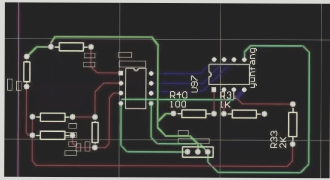
Circuit Analysis
Figure 1 illustrates the schematic diagram of the device, highlighting the MP9486 buck converter chip at its core.
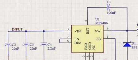
C2, C3, and C4 serve as input decoupling capacitors to minimize voltage noise, with specific placements and functions detailed for each component. The MP9486’s features, including its voltage range, current limit, and control systems, are outlined, emphasizing its suitability for diverse applications.
Essential components like D1, L1, C5, and C6 are discussed for their roles in stabilizing the output and reducing noise, with insights into capacitor types and their impact on circuit behavior. The feedback control loop components are also explained for their contributions to overall stability.
PCB Layout and Assembly
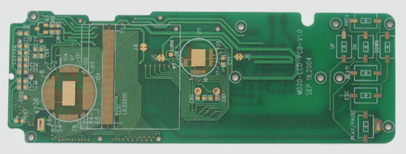
Figure 2 showcases the compact two-layer PCB layout, featuring surface-mount components for efficiency. Assembly drawings in Figure 3 provide further insights into the physical implementation of the design.
PCB Design and Testing: A Comprehensive Overview
When it comes to designing and testing PCBs, one crucial aspect is the layout of the circuit. Take, for example, the 100V to 5V DC-to-DC Buck converter. The PCB layout plays a vital role in ensuring the converter functions efficiently.
Assembly Drawings and Prototypes
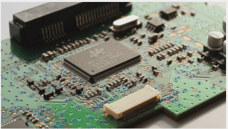
Assembly and testing are key stages in the PCB development process. Figure 4 displays the first revision of the assembled PCB prototype after completion of all tests. For those with time or resource constraints, ordering a pre-assembled board is a convenient option.
The testing phase is critical in verifying the functionality of the PCB. Various tests were conducted, all of which yielded successful results. Detailed testing information can be found in a YouTube video. Additionally, noise measurements under different input and load conditions were taken, as shown in Figures 5 to 8.
Noise Measurements and Oscilloscope
Figure 5 illustrates the output noise of the buck converter with an 8V input and no load. Conversely, Figure 6 depicts the output noise under a 30V input with no load. Furthermore, Figures 7 and 8 showcase the noise levels with maximum load under 8V and 30V inputs, respectively. The Siglent SDS2102X Plus oscilloscope was utilized for these measurements.