Optimizing PCB Assembly for Speed: Key Considerations
When preparing for board assembly, optimizing for speed is crucial for enhanced performance and efficiency. Faster circuit board operation translates to higher work efficiency and increased value in PCB production. Without efficient methods, product delivery delays may occur.
8 Suggestions to Optimize PCB Assembly:
- Plan Ahead: Thoroughly define requirements, analyze signals, and address material needs for efficient assembly.
- Detailed Documentation: Provide comprehensive documentation to suppliers for swift preparation and enhanced efficiency.
- Schematic Design: Focus on minimizing issues and improving efficiency in wiring and design techniques.
- Material and Stacking Requirements: Special materials like Rogers and FR-4 are essential for high-speed boards.
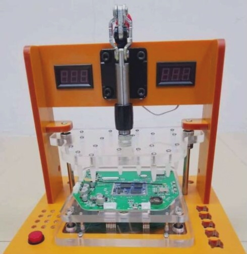
- Component Pick and Place: Adhere to best practices for component placement to enhance overall speed.
- Pad and Pin Size: Pay attention to pad and pin sizes to impact assembly speed and functionality.
- Production Process Collaboration: Effective team communication is crucial for successful high-speed PCB assembly.
Latest Updates:
In the realm of PCB assembly, advancements in materials like Rogers and FR-4 are revolutionizing high-speed board production. These materials play a critical role in stacked structures, significantly impacting PCB performance. By optimizing stacking practices, such as routing high-speed signals on inner layers and utilizing multiple ground planes, manufacturers can achieve faster PCB speeds and more efficient assembly processes.
Enhancing Component Procurement:
Efficient component procurement is key to speeding up PCB assembly processes. Seeking manufacturers who provide quick quotations and turnkey solutions within a short timeframe can streamline sourcing and assembly. Verifying the Bill of Materials (BOM) file before assembly ensures accuracy, avoiding rework and saving valuable time.
Designing for Speed:
When designing PCB layouts, paying attention to pad and pin sizes can significantly impact assembly speed and overall functionality. Communicating effectively with PCB designers to choose simpler designs and optimize space for high-speed circuits is essential. Limiting pad size to a percentage of the component lead size can create more room for critical elements like integrated circuits and FPGAs, ultimately boosting circuit board speed.
Collaboration for Success:
Effective collaboration among team members involved in PCB design and assembly is crucial for achieving high-speed PCB production. Clear communication ensures that design requirements are accurately translated into efficient assembly processes, ultimately leading to successful board operation.
Optimizing PCB Assembly Efficiency
It is crucial to maintain clear communication with your PCB supplier to address any queries promptly. Effective and timely communication plays a significant role in ensuring efficient PCB assembly and minimizing rework. Inform your supplier promptly about any material changes to facilitate quick adjustments.
Choosing the Right Factory Size for Efficient Assembly
Opting for medium to large factories can enhance assembly line efficiency. The size of the factory directly impacts the efficiency of PCB assembly. Medium and large factories typically employ specialized staff in each department, ensuring a high level of professionalism and efficiency.
Ensuring Timely Delivery and Performance
By selecting the right factory size, you can have confidence in meeting deadlines without delays in PCB performance, design, and assembly. Timely PCB assembly is crucial, especially when other processes are dependent on it.
Conclusion
By following the outlined steps, you can optimize the speed and performance of PCB assembly. Careful planning, proper material selection, effective stacking techniques, and ensuring correct pad and pin sizes are all essential factors in achieving high-speed PCB design.