By Hesam Moshiri, Anson Bao
Copyright: Attribution-NonCommercial-NoDerivs (CC-BY-NC-ND)
The power supply is a critical component of any electronic device. Instabilities or failures in the power supply can cause the device to malfunction or exhibit erratic behavior. In this article/video, I present an AC-to-DC flyback switching power supply that converts an input range of 85V-260VAC to a stable 5VDC output at up to 2.5A. This supply is versatile, suitable for a wide range of applications. The 5V output makes it ideal for use with linear regulators that further step down the voltage for specific needs.
The power supply is capable of delivering up to 12W of power, providing a 5V output at a maximum of 2.5A. The controller IC used is the DK1203, which operates without requiring any external power supply, start-up resistors, or an auxiliary winding on the transformer. The transformer features an EE20 ferrite core. A potentiometer is provided to precisely adjust the output voltage to exactly 5.0V.
For the design of the schematic and PCB, I used Altium Designer 23 and shared the project for feedback and revisions via Altium-365. The Octopart component search tool was invaluable for quickly sourcing components and generating the Bill of Materials (BOM). To ensure top-notch board quality, I submitted the Gerber files to Wellcircuits for fabrication.
During testing, I measured voltage drop, current delivery, and output noise. I used a Siglent SDL1020X-E DC Load and a Siglent SDS2102X Plus oscilloscope for the tests. I’m confident that constructing this circuit will deepen your understanding of switching power supply design, and it can also be directly applied in real-world scenarios.
Specifications
Input Voltage: 85-265VAC
Output Voltage: 5VDC
Maximum Output Current: 2.5A
Maximum Continuous Output Current: 2A
Output Noise (No load): 1.5mV (rms), 4mV (p-p)
Output Noise (Max Load, 2A): 3mV (rms), 25mV (p-p)
Maximum Voltage Drop (2A load): 50mV
Transformer Type: EE20
Download the Gerber files or order 10 high-quality boards for just $5
If you’d like to order a fully assembled PCB (with free shipping), just click here
Circuit Analysis
Figure 1 illustrates the schematic of the flyback switching power supply. The core component is the DK1203 controller chip [1].
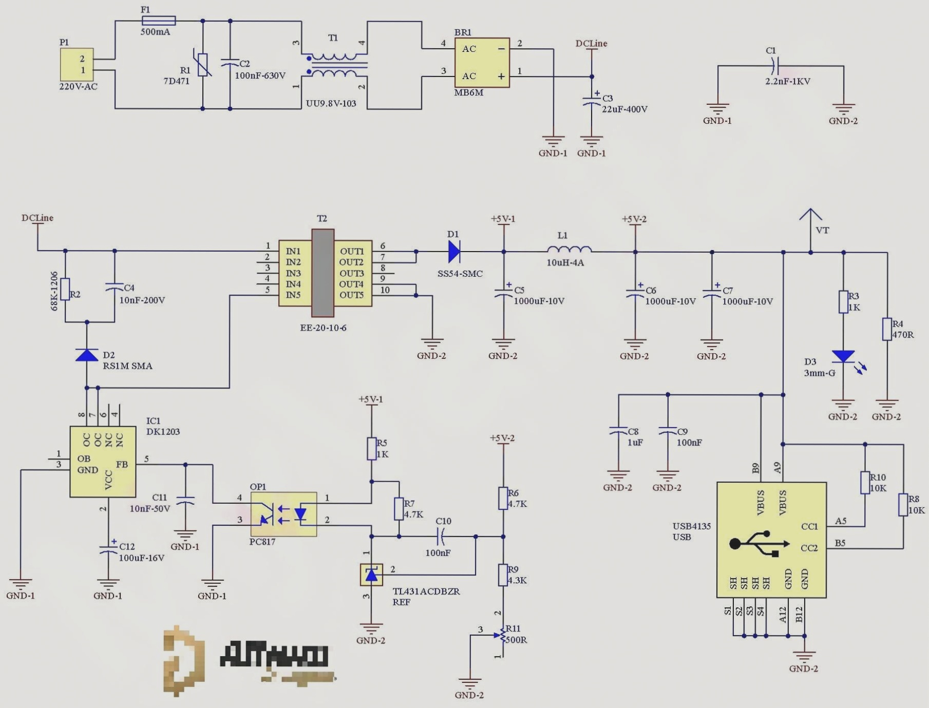
Figure 1
Schematic diagram of the flyback switching power supply
P1 is the input terminal for the AC voltage, with a wide input range of 85V to 260V AC, capable of delivering up to 12W of output power within this range. F1 is a 500mA fuse [2], and R1 is a 7D741 varistor [3] used to absorb voltage transients. C2 is a 100nF X2-rated capacitor [4] for reducing high-frequency noise, while T1 is a common-mode choke [5]. BR1 is a Vishay MB6M bridge rectifier [6], and C3 is a 22uF-400V capacitor [7] that reduces voltage ripple.
R2, C4, and D2 make up the snubber circuit, which dampens switching spikes. D2 is an RS1M SMA [8] diode. The switching controller is the DK1203, and OP1 is a PC817 [9] optocoupler, which allows the controller to sense and stabilize the output voltage. REF is the TL431 shunt regulator [10] that stabilizes the output and transfers any fluctuations to the optocoupler.
D1 is an SS54 SMC [11] Schottky diode, which rectifies the output voltage. C5, C6, C7, and L1 work together to reduce output noise. R4 is a 470Ω 1206 resistor [12], providing a preliminary load to stabilize the output. D3 is a 3mm red LED, which indicates proper operation of the power supply and output voltage. C8 and C9 reduce high-frequency noise. VT is a test point (a single male pin header) where you can connect a multimeter to read the output voltage. The R11 potentiometer is used to fine-tune the output to a precise 5.0V.
The USB connector, USB4135 Type-C, is used to connect an external USB Type-C cable to power your devices.
PCB Layout
Figure 2 shows the PCB layout for the switching power supply. It is a two-layer PCB design with a combination of SMD and through-hole components.

Figure 2
PCB layout of the flyback AC-DC switching power supply
Transformer Design
To build the transformer, follow these steps:
Core: Ferrite, EE-20-10-6 (B66311G0000X187)
Primary Winding: 2.88mH (124 turns of 0.2mm wire)
Gap: approximately 0.25mm (mathematically calculated)
Secondary Winding: 6 turns of 2 x 0.7mm wires (two 0.7mm wires in parallel)
Bobbin: 5+5, E20 Horizontal (B66206B1110T001)
Typically, EE cores come without a gap (between the two central legs of the core), so you’ll need to grind the middle legs to create a gap. However, this process requires precision, and it can be difficult to achieve the correct gap by hand.
A simpler approach is to use an LCR meter. First, wind the primary and assemble the transformer without the gap. Measure the inductance of the primary winding; it will likely exceed 2.88mH. Grind the center leg to create a gap, then reassemble the transformer and remeasure the inductance. Repeat this process until the inductance reaches 2.88mH. A small tolerance from 2.88mH is acceptable and won’t affect performance. Figure 3 shows the EE core and the gap.
Figures 4 and 5 show the ferrite core and the winding process for the transformer.

Figure 3
The EE20-10-6 core and the non-magnetic gap in the center
Post navigation

