How to Make a PCB: A Step-by-Step Guide
Designing a PCB is a crucial process that requires attention to detail at every step to avoid costly mistakes. Here is a comprehensive guide on how to make a PCB:
Why Design a PCB First?
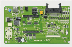
Before delving into the PCB fabrication process, understanding the basics of a Printed Circuit Board is essential. A PCB serves as an insulating base with patterns of conduction components. Whether your project is simple or complex, designing a PCB first is crucial to determine component placement and avoid delays and additional costs.
Guideline on How to Make a PCB
Starting a PCB project requires a clear guideline to ensure success. Here are the steps you need to follow:
1. Knowledge of Electrical Parameters
Prioritize understanding the electrical parameters of your PCB, including signal types, voltages, current maximums, impedance characteristics, capacitance limitations, circuit components, connectors, and net wiring.
2. Schematic File
Sort out the electrical parameters before creating a schematic file. This file will outline the design details of your PCB, specifying the board’s function, purpose, and equipment compatibility.
3. Preparing a Schematic
Utilize software tools to create a schematic that details the electrical components, connections, and relationships between components. This step serves as a prototype for the actual PCB construction.
4. PCB Layout
Once the schematic is ready, use a schematic capture tool like Altium Designer to import components into a blank PCB document. Define the PCB dimensions, shape, and layer stack up to create a PcbDoc file for verification and project documentation.
5. Design a PCB Stack-Up

PCB Design Guide: Essential Steps to Create a Printed Circuit Board
When transitioning from the schematic to the PcbDoc, the component footprints appear on the board outline, involving component placement and defining the PCB layout.
Modern PCB Design Concepts
For first-time PCB designers, starting with a 4-layer board on FR4 is common, but the design can vary based on project requirements. It’s crucial to establish PCB DFM requirements and design rules.
Important Rules for PCB Design
-
Object Clearances:
Clearances between pads and traces in the PCB layout.
-
Copper and Solder Mask Limits:
Size limits of copper or solder masks, including solder mask silvers and holes.
-
Routing Rules:
Width and length limitations of routing rules.
-
Signal and Speed Constraints:
Limits related to signal integrity and high-speed design.
-
Fabrication Limits:
Restrictions concerning board fabrication and clearances.
Placing Components on the PCB
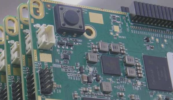
Now it’s time to position components on the PCB. You have the option to manually or automatically place elements on the board. While manual placement offers control, automatic placement can save time. After automatic placement, ensure manual verification following PCB design guidelines.
Drilling Holes
Drill holes according to the PCB design complexity, simplifying where possible for clarity.
Routing Traces
After component placement, proceed with routing traces, focusing on essential routes like power nets, noise-sensitive nets, and impedance-controlled nets. Fill gaps strategically to optimize the layout.
Component Identification and Labeling
Once the PCB layout is set, identify components with clear labels to avoid misplacement. These identifiers aid in assembly and debugging, ensuring components are correctly positioned.
Incorporate company logos for professional projects, enhancing the PCB’s branding.
Generating Output Files
Before ordering PCB components, verify all details to rectify any errors. Utilize tools like Altium Designer for automatic verification. Generate a design file for self-assembly or manufacturing, including special notes and requirements for reference.
Ready to Begin
The comprehensive PCB design guide comprising 10 crucial steps is now complete. Follow each step meticulously to avoid errors during the design process. Whether self-assembling or outsourcing, retain the prepared file for validation purposes.
Essential Tips for Successful PCB Design
Mastering the art of PCB design is crucial for creating flawless electronic devices. To ensure a smooth process, remember these key points:
- Follow each step meticulously to avoid costly mistakes.
- Double-check every detail to prevent having to restart the project.
- Time and money can be saved by adhering to the guidelines.
Whether you prefer a DIY approach or seek professional assistance, sharing your PCB design requirements with experts at Well Circuits can streamline your project.