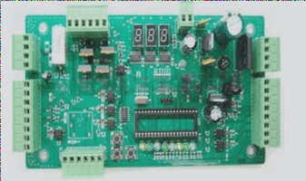
Revolution of PCBs in Electronics
Printed Circuit Boards (PCBs) have transformed the electronics industry by providing a way to convert temporary circuits into permanent, professional-looking designs. Initially limited to through-hole components, PCB technology has advanced to accommodate Surface Mount Devices (SMD) for circuits of all sizes.
The Essential Steps in PCB Fabrication
Before delving into the specifics of PCB printing, understanding the fundamental PCB manufacturing steps is crucial. While some tasks are best left to professionals, beginners can handle certain aspects with care.
Step 1: Create Your Electrical Design
Begin by drafting a schematic using PCB software like Eagle or EasyEDA. This schematic serves as the blueprint for your PCB layout, guiding component placement and connections.
Step 2: Verify Your Design
After translating your schematic into a layout, perform a thorough check, ensuring correct pad positioning and trace routing. Pay attention to trace widths, especially for components like ICs, to maintain optimal performance.

Step 3: Printing Your PCB
To print your PCB, gather materials such as butter paper, A4 toner paper, a copper plate, and an inkjet printer. Follow these steps:
- Print your layout onto the toner paper.
Latest Developments in PCB Technology
Recent advancements in PCB fabrication include the integration of flexible and rigid-flex PCBs, enabling innovative designs for wearable tech and IoT devices. Additionally, the rise of eco-friendly PCB materials reflects a growing emphasis on sustainability in electronics manufacturing.
Essential Steps for Printing Your PCB Design
- Resize the image
Once you have created your PCB design, the next crucial step is to save it in the right format. Most PCB design software offers options like saving as a PDF or exporting as an image. Choose the Save as PDF option or a similar one to download your PCB layout.
After saving the design, print it on butter paper using an inkjet printer. Ensure to print on the shiny side of the paper for better results.
Why Removing Copper from the Board is Important
It is essential to remove excess copper or resist from the board to ensure a clear and precise image transfer. Excess copper can interfere with the printing process and lead to issues during etching.
Step 4: Transfer the PCB Layout
Transfer the resized PCB print onto the copper board by aligning and pressing it with a hot iron. Be cautious with the iron’s temperature and pressure to avoid damaging the paper or the board.
Step 5: Masking the Copper Traces
If any traces are incomplete after transferring the layout, use a permanent marker to fill in the gaps. This process, known as masking, ensures all traces are properly transferred.
Step 6: Etching Process
With proper safety precautions, immerse the printed circuit board in a ferric chloride solution for about 30 minutes. The solution reacts with the unmasked copper, etching away the excess metal. Monitor the process carefully and adjust if needed for optimal results.
Post-Printing Tasks for Your PCB
After completing the printing and etching process, the next step involves drilling holes in the PCB using a specialized drilling machine. This step is crucial for accommodating the electronic components on the board securely.
PCB Plating Process: A Crucial Step in PCB Printing
- PCB plating is a critical step in the PCB printing process, following the initial learning phase. This step involves covering the PCB board with a micron-thick layer, strategically placed between the drilled holes for enhanced conductivity.
- The final etching process is equally essential in mastering the art of PCB printing with precision and accuracy.
- This step aids in removing excess copper, thereby reinforcing the connections on the printed circuit board. By completing this step, you can ensure that the PCB is well-prepared for the subsequent soldering process.
Subsequently, the soldering mask application emerges as a pivotal stage in the PCB printing journey. During this phase, a solder mask is applied to the PCB, followed by exposure to ultraviolet rays. This crucial process contributes to the durability and strength of the printed circuit board.
In Closing
The process of PCB printing is no longer shrouded in mystery. With the right guidance and adherence to the prescribed steps, mastering PCB printing is within reach, even for beginners or those uncertain about where to commence. Therefore, if you find yourself feeling anxious or uncertain, rest assured that we have the expertise to support you every step of the way.