
HDI PCB: Revolutionizing High-Density Interconnect Technology
HDI (High Density Interconnect) PCBs are at the forefront of PCB innovation, offering unparalleled wiring density compared to traditional designs. These boards utilize buried/blind vias and microvias as small as 0.006 inches, along with ultra-thin high-performance materials and fine wiring, making them indispensable in critical industrial applications.
1. Exploring HDI PCB Microwells
The enhanced wiring density of HDI PCBs allows for more functions within a confined space. Advanced HDI PCBs feature stacked microvias filled with multilayer copper, enabling intricate interconnections. Microvias, drilled with lasers, facilitate interconnection across layers in circuit boards, especially in advanced smartphones and handheld devices.
2. Diving into Types of HDI PCBs
- HDI PCB (1+N+1): These boards incorporate a “stacked” high-density interconnect layer, offering stability and easy installation. Ideal for applications like mobile phones, MP3 players, and GPS devices.
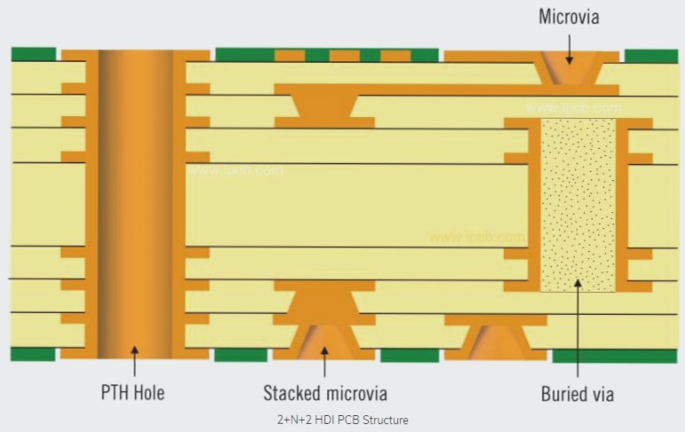
HDI PCB (2+N+2):
Featuring multiple stacked microvia layers, these PCBs utilize low Dk/Df materials to enhance signal performance, making them perfect for devices like PDAs, camcorders, and mobile phones.
ELIC (Each Layer Interconnection):
ELIC PCBs boast high-density interconnection layers across the board, allowing for free conductor interconnection via stacked copper-filled microvias. Widely used in GPU chips, CPUs, and memory cards.
Advantages of HDI PCBs:
HDI PCBs offer a cost-effective alternative to standard laminates for high-layer configurations, thanks to their numerous advantages.
Laser Drilling Insights:
In HDI mobile phone boards, microvia blind holes are typically 0.1mm in diameter. CO2 lasers are used for drilling, with a unique process for etching copper layers after drilling to maintain copper integrity.
Plugging and Solder Mask Application:
For HDI laminate configurations, precise instructions are followed for plugging holes and applying solder mask ink, especially around vias close to SMDs to prevent ink exposure or oil leakage.
When vias cannot be removed, a specific process involving light transmission points on the solder mask layer is implemented for optimal results.
Improving PCB Design for HDI Mobile Phones
One common practice in PCB design is to add a light transmission point 3 MIL larger than one side of the finished hole on the solder mask layer at the through-hole position of the solder mask opening touch. This slight adjustment, although accepted by customers, can enhance the overall quality of the PCB.
When it comes to designing HDI mobile phone PCBs, CAM production personnel face challenges due to the complex shapes and high wiring densities involved. Meeting customer demands for high quality and quick delivery requires continuous practice and knowledge sharing among CAM colleagues to ensure accurate and timely production.