**1. Automatic Push Function in PCB Routing**
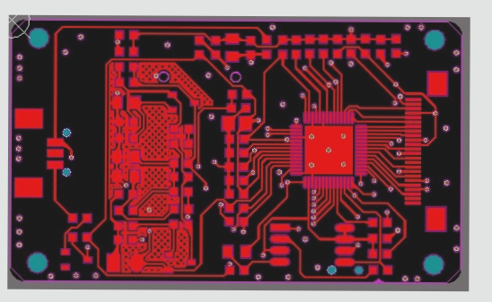
The PCB offers a highly useful function known as automatic push. When we manually route the PCB, we have full control over the layout. However, once the automatic push function is enabled, it becomes much more convenient to optimize the routing process.
If you plan to use automatic routing after completing the initial pre-routing, it’s essential to secure the pre-arranged traces. Otherwise, the software may interpret these segments as movable, potentially disrupting your design and causing unnecessary setbacks.
**4. Adding Positioning Holes**
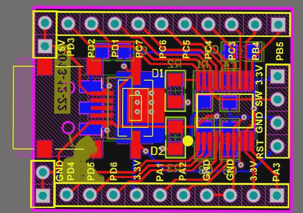
Printed circuit boards often require mounting positioning holes, but for tools like POWERPCB, these holes are considered separate devices from the schematic and must be added in eco mode. If errors arise during the final verification, it can be quite inconvenient.
To avoid this, you can configure the positioning hole device as non-eco registered. In the “Edit Device” window, click the “Edit Electrical Properties” button, ensuring that the normal option is selected while the ECO-registered option is left unchecked.
**5. Adding a New Power Pack**
During the inspection, POWERPCB believes there is no need to compare the device with the netlist, as errors that shouldn’t occur will not appear.
To add a new power pack, we recognize that many international and U.S. software companies are not fully compliant with the standards. Therefore, we try to equip the international library for universal use. However, new symbols for power and ground must be included in the software’s library, otherwise the symbol you create will not be recognized as a power source. To build a power symbol that complies with GB standards, you need to open the existing power symbol group, click the “Edit Electrical Connection” button, then click the “Add” button, and enter the new symbol name and other details. Next, click the “Edit Door Encapsulation” button, select the newly created symbol, draw the desired shape, exit the drawing mode, and save your changes. You can then use the new symbol in your schematic.
**6. Setting Empty Pins**
In the components we use, some pins are designated as empty and are marked as NC. When building a library, it’s important to be cautious about these pins. If you don’t handle them properly, pins marked as NC might unintentionally connect to others. This issue arises because when building the library, NC pins are placed in the “Signal_pins” group, where POWERPCB treats them as implicit default pins. These pins are usually functional, such as VCC or GND.
Therefore, NC pins should be removed from “Signal_pins”. More precisely, they should not be included in the first place, as there is no special definition for them.
**7. Transistor Pin Control**
The packaging of transistors has evolved significantly. When creating your own transistor library, it’s common to find that the connection between the web table and the PCB schematic does not match your intended configuration. The problem typically arises from the database construction. Since transistor pins are usually labeled as E, B, and C, when creating your transistor library, you should check the “Include text numbered pins” option in the edit electrical connection window. This will enable the text-numbered pins tab to highlight. Once you input the label, the corresponding transistor pin will be displayed as a letter.
This approach will make it easier to identify the correct PCB package for the transistor connection.
**8. Preprocessing of Surface-Mounted Devices (SMD)**
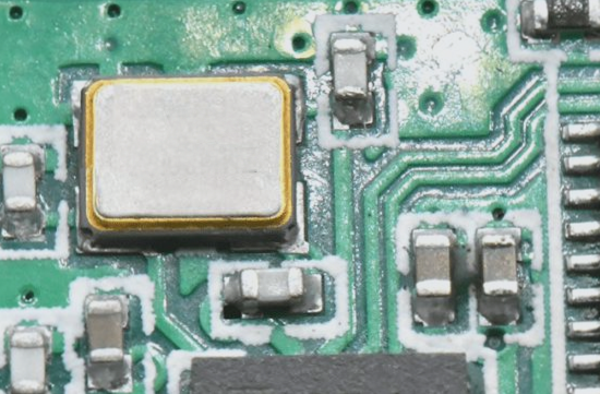
With the increasing demand for miniaturization, surface-mount devices (SMDs) are becoming more common. Handling these devices correctly during the layout process is crucial, especially when working with multilayer boards. Unlike through-hole components, which have connections on both sides, surface-mounted devices connect electrically to only one layer. If a connection to another layer is needed, a short trace is drawn from the device’s pin, and a via hole is created to make the connection to other components. This process is referred to as “fan-in” (for connections coming in) and “fan-out” (for connections going out).
If necessary, start by performing the fan-in and fan-out operations before laying out the traces. If you rely solely on automatic routing settings, the software will perform the fan-in and fan-out during the routing process, resulting in longer and more convoluted traces. To avoid this, complete the PCB layout first, then enter the auto-routing setup. Select only the fan-in and fan-out operations in the configuration file, without selecting other routing options. This ensures the trace from the surface-mounted device is shorter and cleaner.
If your have any questions about PCB ,please contact me info@wellcircuits.com

