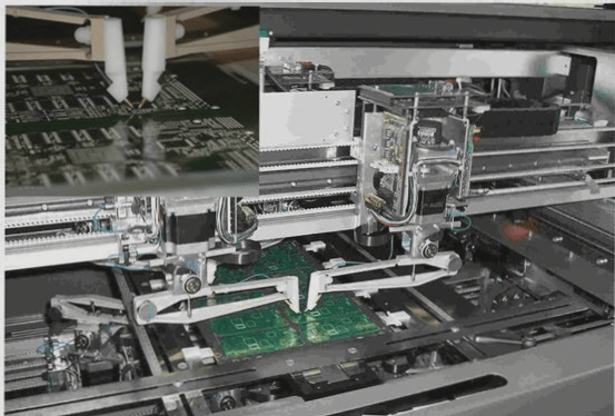
Application of Acid Copper Plating in PCB Manufacturing
After a series of processes, the printed circuit board (PCB) needs to be metallized and copper needs to be deposited on the hole wall surface of the through hole. This ensures interconnection between boards and facilitates strong conductivity. Copper is considered the most widely used material for deposition in the industry. Typically, the metallization process for holes involves two steps: electroless plating and electroplating.
Electroless Plating
Electroless plating, also known as chemical copper precipitation, is a process where copper is deposited onto the PCB through a chemical reaction. This reaction is self-catalyzed, meaning it continues due to the generation of copper atoms and hydrogen atoms, facilitating the reaction towards completion.

The quality of the electroless plating copper layer is critical to achieving optimal PCB performance. Strict control over experimental conditions and operational specifications during the electroless plating process is essential, such as time, temperature, and solution quality. Inadequate solution fluidity and contamination can directly impact the copper plating quality. If the plating solution has poor fluidity, it may lead to an uneven copper layer and result in the formation of voids in the through-holes, posing challenges for subsequent plating steps. To ensure uniform plating, the PCB is typically moved from side to side, and air pumping is used to improve solution flow.
Electroplating Technology
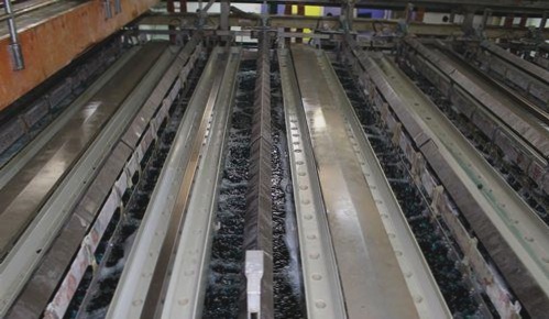
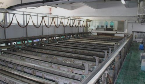
In the copper electroplating industry, sulfate-based systems are commonly used. The figure below illustrates the principle of copper deposition in a cupric acid electroplating system. As the DC power supply is applied, the ions in the solution move toward the cathode, where copper ions (Cu²⁺) are reduced and deposited onto the cathode surface, including the inner walls of the through-holes, forming a copper plating layer.

During this electrochemical reaction, copper ions (Cu²⁺) from the solution are reduced at the cathode, forming copper (Cu) that adheres to the cathode surface and through-hole walls. Over time, as the copper ions are consumed, the anode dissolves to replenish the copper ion concentration, maintaining the balance of the plating solution.

This cyclic process of copper consumption at the cathode and replenishment at the anode ensures that the electroplating process remains balanced and continuous.
Understanding Electroplating Reactions in PCB Manufacturing
Electroplating reactions in PCB manufacturing involve a two-step process. Initially, reactions produce an intermediate that leads to the desired product, such as the deposition of a copper layer.

During the plating process, the decrease in certain ion concentrations can lead to hydrolysis reactions if oxidation is insufficient. This can impact the quality of the copper plating surface on the PCB.

Continued hydrolysis due to decreasing acid concentration can create burrs on the cathode plate, affecting performance. Monitoring and replenishing acid levels are crucial to prevent this issue.

Additives in the electroplating system influence current density and crystal growth rate, impacting the quality of the copper deposit. Monitoring additive consumption and replenishing them in real time is essential for successful deposition.
Consumption of additives during electroplating can lead to irreversible reactions with the anode, affecting additive concentration and deposit quality. Real-time monitoring and replenishment are necessary to ensure optimal results.

If you have any questions about PCB and PCBA, please feel free to contact me at info@wellcircuits.com.