1. The traditional tools for debugging PCB boards include time-domain oscilloscopes, TDR (time-domain reflectometry) oscilloscopes, logic analyzers, and frequency-domain spectrum analyzers. However, none of these methods can provide a comprehensive overview of the PCB board data.
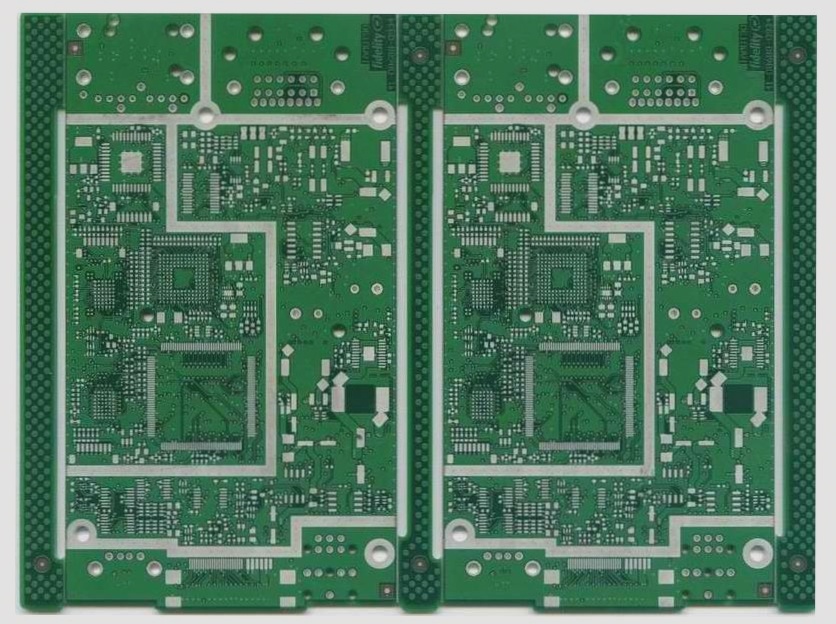
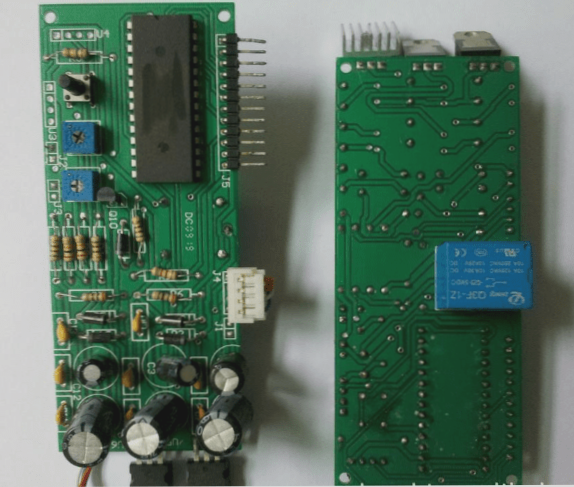
2. A PCB board, also known as a printed circuit board or printed wiring board (abbreviated as PCB or PWB), uses an insulating board as the base material. It is cut into a specific size and contains at least one conductive pattern with holes (such as component holes, fastening holes, metallized holes, etc.). These boards replace the chassis of traditional electronic components and facilitate interconnections between them. Due to their manufacturing process involving electronic printing techniques, they are called “printed” circuit boards. It’s important to note that a “printed circuit board” should not be confused with a “printed circuit” since the former contains wiring but not printed components.
3. The Emscan electromagnetic compatibility scanning system employs advanced array antenna technology and electronic switching technology to measure the current of PCBs rapidly. The core of Emscan lies in its array antenna, which assesses the near-field radiation of a functioning PCB positioned on the scanner. The antenna array comprises 1280 small H-field probes arranged in a 40 x 32 configuration on an 8-layer circuit board with a protective layer designed to accommodate the PCB under test.
4. The results of the spectrum scan provide a general overview of the emissions from the Equipment Under Test (EUT), indicating the number and approximate magnitude of frequency components present.

Full frequency scan
The design of the PCB board is based on the circuit schematic diagram to realize the functions required by the circuit designer. The design of the printed circuit board mainly refers to the layout design, which needs to consider various factors such as the layout of external connections, the optimal arrangement of internal electronic components, metal connections, and through holes, as well as considerations for electromagnetic protection and heat dissipation. Effective layout design can reduce production costs while achieving optimal circuit and heat dissipation performance. Simple layouts can be done manually, while complex designs require computer-aided design.
When performing spectral/spatial scans, place the PCB on the scanner. The scanner divides the PCB into 7.6mm*7.6mm grids (each containing an H-field probe). It scans each probe across the full frequency range (from 10kHz to 3GHz). Emscan produces two images: a synthetic spectrogram and a synthetic spatial graph. Spectral/spatial scans capture spectral data across the entire scan area, enabling quick localization of electromagnetic interference sources.
A spectrum analyzer is essential for studying the spectral characteristics of electrical signals, measuring parameters like signal distortion, modulation, spectral purity, frequency stability, and intermodulation distortion. It serves various purposes in circuit analysis, resembling a frequency domain oscilloscope, tracking oscilloscope, or harmonic analyzer. Modern spectrum analyzers cover a wide range of radio frequencies, from below 1 Hz to sub-millimeter bands, displaying results digitally or in analog form.
Using a spectrum analyzer and single near-field probe, engineers can pinpoint sources of electromagnetic interference, akin to identifying the origin and path of a fire. Traditional methods are akin to detecting flames escaping from a chassis, while EMSCAN allows detection of interference sources (“kindling”) and their transmission paths (“fires”). This method efficiently resolves EMI/EMC issues by accurately tracing sources and propagation paths.
To quickly pinpoint circuit faults, particularly as PCB complexity increases, engineers face challenges in observing numerous signal lines simultaneously using oscilloscopes or logic analyzers. Comparing electromagnetic data between a normal and faulty PCB can reveal abnormal frequency spectra. Utilizing interference source location technology identifies where these abnormalities occur spatially, facilitating rapid diagnosis and resolution of faults.
Assessing PCB design quality involves several critical factors: rational stacking design, minimizing signal line impedance disruptions, effective power supply filtering, ensuring ground plane integrity, and balancing signal integrity with electromagnetic compatibility. Evaluating PCB design comprehensively using electromagnetic field data helps optimize performance and reliability.
In summary, comprehensive electromagnetic information enhances engineers’ ability to solve EMI/EMC problems, debug PCBs effectively, and continually enhance PCB design quality.
2. A PCB board, also known as a printed circuit board or printed wiring board (abbreviated as PCB or PWB), uses an insulating board as the base material. It is cut into a specific size and contains at least one conductive pattern with holes (such as component holes, fastening holes, metallized holes, etc.). These boards replace the chassis of traditional electronic components and facilitate interconnections between them. Due to their manufacturing process involving electronic printing techniques, they are called “printed” circuit boards. It’s important to note that a “printed circuit board” should not be confused with a “printed circuit” since the former contains wiring but not printed components.
3. The Emscan electromagnetic compatibility scanning system employs advanced array antenna technology and electronic switching technology to measure the current of PCBs rapidly. The core of Emscan lies in its array antenna, which assesses the near-field radiation of a functioning PCB positioned on the scanner. The antenna array comprises 1280 small H-field probes arranged in a 40 x 32 configuration on an 8-layer circuit board with a protective layer designed to accommodate the PCB under test.
4. The results of the spectrum scan provide a general overview of the emissions from the Equipment Under Test (EUT), indicating the number and approximate magnitude of frequency components present.

Full frequency scan
The design of the PCB board is based on the circuit schematic diagram to realize the functions required by the circuit designer. The design of the printed circuit board mainly refers to the layout design, which needs to consider various factors such as the layout of external connections, the optimal arrangement of internal electronic components, metal connections, and through holes, as well as considerations for electromagnetic protection and heat dissipation. Effective layout design can reduce production costs while achieving optimal circuit and heat dissipation performance. Simple layouts can be done manually, while complex designs require computer-aided design.
When performing spectral/spatial scans, place the PCB on the scanner. The scanner divides the PCB into 7.6mm*7.6mm grids (each containing an H-field probe). It scans each probe across the full frequency range (from 10kHz to 3GHz). Emscan produces two images: a synthetic spectrogram and a synthetic spatial graph. Spectral/spatial scans capture spectral data across the entire scan area, enabling quick localization of electromagnetic interference sources.
A spectrum analyzer is essential for studying the spectral characteristics of electrical signals, measuring parameters like signal distortion, modulation, spectral purity, frequency stability, and intermodulation distortion. It serves various purposes in circuit analysis, resembling a frequency domain oscilloscope, tracking oscilloscope, or harmonic analyzer. Modern spectrum analyzers cover a wide range of radio frequencies, from below 1 Hz to sub-millimeter bands, displaying results digitally or in analog form.
Using a spectrum analyzer and single near-field probe, engineers can pinpoint sources of electromagnetic interference, akin to identifying the origin and path of a fire. Traditional methods are akin to detecting flames escaping from a chassis, while EMSCAN allows detection of interference sources (“kindling”) and their transmission paths (“fires”). This method efficiently resolves EMI/EMC issues by accurately tracing sources and propagation paths.
To quickly pinpoint circuit faults, particularly as PCB complexity increases, engineers face challenges in observing numerous signal lines simultaneously using oscilloscopes or logic analyzers. Comparing electromagnetic data between a normal and faulty PCB can reveal abnormal frequency spectra. Utilizing interference source location technology identifies where these abnormalities occur spatially, facilitating rapid diagnosis and resolution of faults.
Assessing PCB design quality involves several critical factors: rational stacking design, minimizing signal line impedance disruptions, effective power supply filtering, ensuring ground plane integrity, and balancing signal integrity with electromagnetic compatibility. Evaluating PCB design comprehensively using electromagnetic field data helps optimize performance and reliability.
In summary, comprehensive electromagnetic information enhances engineers’ ability to solve EMI/EMC problems, debug PCBs effectively, and continually enhance PCB design quality.


