Challenges Faced by PCB Manufacturers
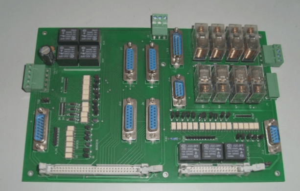
Printed circuit board (PCB) manufacturers are under pressure to increase density, reduce size, manage heat, enhance data transfer rates, and improve reliability while cutting costs. One emerging issue is aligning multiple pairs of connectors between PCBs.
Guidelines for Effective Alignment
Clear guidelines are needed to tackle alignment challenges without compromising system performance, density, or reliability. Designers must also adhere to tight budget constraints and accelerated time-to-market demands.
Deeper Dive into Alignment Challenges
This article explores alignment challenges between advanced PCBs and high-density connectors. It offers design practices to efficiently meet these demands.
Miniaturization Impact on Connector Alignment
Miniaturization poses challenges for PCB designers when selecting and implementing connectors, especially with multiple connectors on a single PCB. Over the years, connector spacing has significantly decreased, demanding tighter tolerances and careful alignment considerations.
- Miniaturization has led to a six-fold reduction in connector spacing over 25 years.
- Variances in tolerances can lead to alignment issues between connectors.
- Designers must consider tolerances across all components for successful integration.
Addressing Alignment Issues
For multi-connector applications, designers need to supplement Gerber files with mechanical drawings specifying tolerances. Engaging with suppliers and conducting tolerance studies are crucial steps to ensure successful alignment.
- Engage with PCB and connector suppliers for alignment support.
- Conduct system-level tolerance studies to assess alignment deviations.
- Compare connector specifications with tolerance study results to ensure reliability.
Importance of Communication with Connector Manufacturers
Maintaining communication with connector manufacturers is essential to validate alignment deviation tolerances and prevent costly errors. Positioning pins may not be ideal for multi-connector applications.
Positioning Pins in Connector Manufacturing
Some manufacturers of connectors provide optional positioning pins, usually located at the bottom of the connector on opposite sides (refer to Figure 4). These pins are designed to aid in manual placement, assist in aligning the connector on the PCB, and do not add to the overall tolerance stack-up in single-connector scenarios.
It is important to note that while positioning pins can be beneficial in certain situations, they may not be suitable for multi-connector applications. In cases where precise alignment and tolerance control are crucial for the success of the project, alternative methods should be considered.
If you have any inquiries regarding PCBs, feel free to reach out to us at info@wellcircuits.com.