Constructing a High-Performance Power Supply with TPS54202 Chip
Authors: Hesam Moshiri, Anson Bao
License: CC-BY-NC-ND
A power supply is an essential tool in electronics labs. The TPS54202 is a 2A synchronous buck converter known for its efficiency, wide input voltage range, and low EMI. These features make it ideal for various applications, ensuring reliable performance for your projects.
Implementing input and output filters, along with PCB design techniques, helps minimize noise and optimize performance. Operating at 500 kHz, the chip includes internal loop compensation for ease of setup. Simply connect the input to a step-down AC transformer (e.g., 220V to 15V) and adjust the output voltage using a multiturn potentiometer.
For schematic and PCB design, Altium Designer 23 was utilized, with project sharing via Altium-365. The Octopart component search engine facilitated component sourcing and BOM generation. Gerber files were sent to Wellcircuits for high-quality board production.
Specifications:
- Input Voltage: Up to 20V AC
- Output Voltage Range: 0.6V DC to VTR-1
- Max Continuous Output Current: 2A
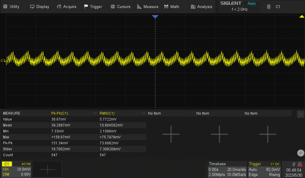
- Output Noise (No Load): 3mV(rms), 16mV(p-p)
- Output Noise (Max Load): 6mV(rms), 30mV(p-p)
- Max Voltage Drop at Full Load: 100mV
Circuit Analysis:
Figure 1 displays the schematic diagram of the adjustable switching power supply utilizing the TPS54202 chip as the core component. Input capacitors C2, C3, C4, and C5 reduce noise, with proper placement order critical for effectiveness. L1 is a 22μH inductor, and R2 is a 5K multiturn potentiometer for voltage adjustment.
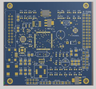
PCB Layout:
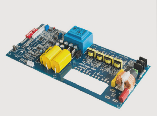
Figure 2 showcases the PCB layout of the project, a double-layer board with surface-mount components. Refer to the YouTube video for PCB design techniques. Assembly drawings are depicted in Figure 3.
Adjustable Low EMI Switching Power Supply Project
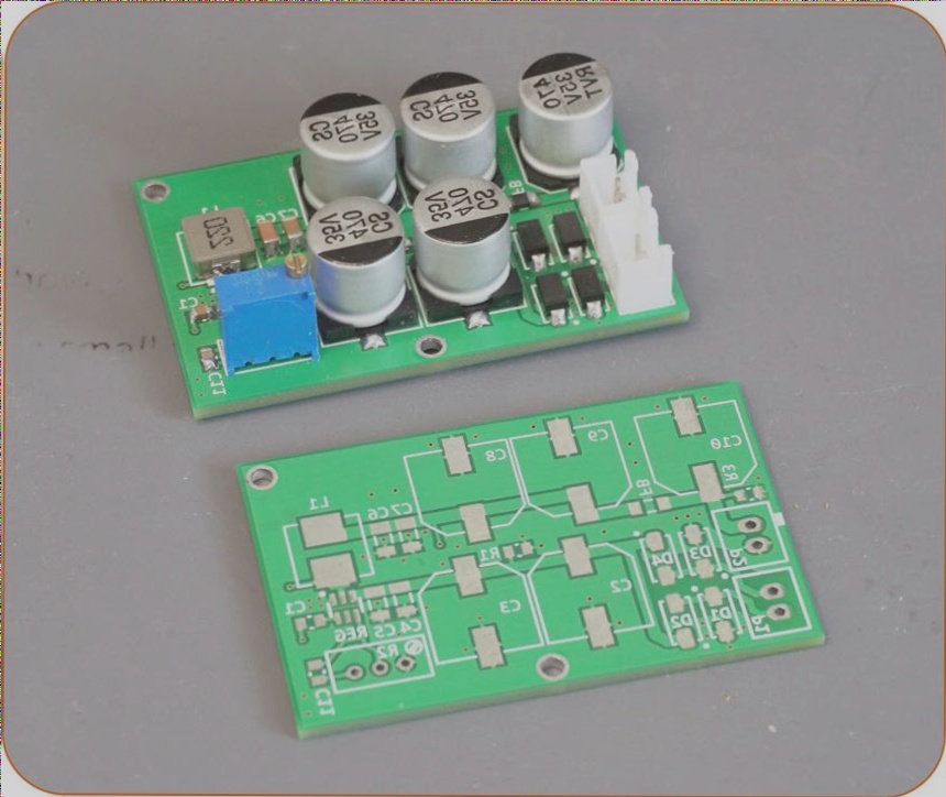
When assembling the PCB board for the adjustable low EMI Switching Power Supply project, soldering the TPS54202 (REG) component may require precision. Using a microscope can aid in this process, but manual soldering is also feasible. If soldering isn’t your preference, you have the option to order the board pre-assembled.
Assembled PCB Board
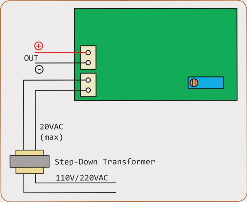
Connection Diagram
For the power supply, refer to the connection diagram shown in Figure 5 below:
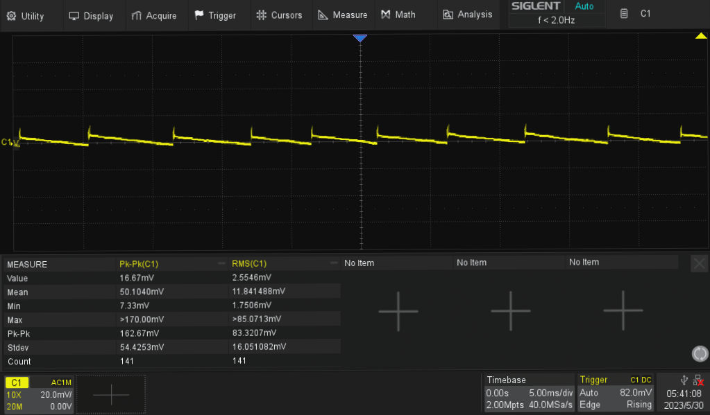
Output Noise and Performance
Figure 6 displays the output noise of the power supply with no load, analyzed using the Power Analysis feature of the Siglent SDS2102X Plus oscilloscope. Additionally, Figure 7 showcases the output noise under maximum load (2A). In case of unsatisfactory noise levels, pay attention to the significant input ripple at the controller input, depicted in Figure 8. Lastly, Figure 9 reveals the results of the step response test, demonstrating the power supply’s stability, recovery time, and performance under varying loads.
Output Noise Analysis
Performance under Maximum Load