The source material for this blog post is sourced from https://www.ti.com/lit/an/slva773/slva773.pdf.
PCB Designs
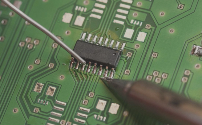
PCB layout is a critical aspect of high-level engineering in circuit board design. It involves intelligent hand routing for high-speed and differential signals, as well as utilizing auto-routers based on shape or advanced configuration options for large-scale import/export. Real-time Design Rule Checking (DRC) is a key feature in PCB design tools like DipTrace, which automatically detects and reports errors during the design process. Designers can also visualize their boards in 3D, which aids in CAD modeling for mechanical integration. The final product quality is ensured by validating design rules, verifying net availability, and conducting thorough analysis, with a final comparison to the source schematic.
A boost converter is a basic form of switch-mode power supply (SMPS) that increases the input voltage. It consists of a capacitor, a microelectronics switch, an inductor, and a transistor, along with a standard square wave oscillator. Unlike bulky AC transformers, the simplicity of the boost converter allows it to be lightweight and efficient—originally designed for military aircraft equipment in the 1960s. One of its key advantages is its high efficiency, with some designs achieving up to 99% energy conversion, meaning that only 1% of the input energy is lost.
Working of the Boost Converter
To fully understand the operation of a boost converter, it’s important to grasp the function of its key components: inductors, MOSFETs, transistors, and capacitors.
1. The internal transistor begins by charging the capacitor.
2. Once the power is turned on, the MOSFET switches on when the signal source rises. This reroutes current through the MOSFET, while the external capacitor remains fully charged because it cannot discharge through the now back-biased inductor. The inductor delays the ramp-up of current to prevent an immediate short circuit. A magnetic field forms around the capacitor, and the input power remains polarized.
3. When the MOSFET is switched off, the inductor’s current is abruptly interrupted. Inductors resist rapid changes in current and maintain current flow by using the stored energy in the magnetic field. This forces the current to flow in the reverse direction, gradually transferring energy. As the current increases, the transistor’s anode becomes more positive, raising the voltage across the output capacitor. This process boosts the DC voltage from a lower to a higher level.
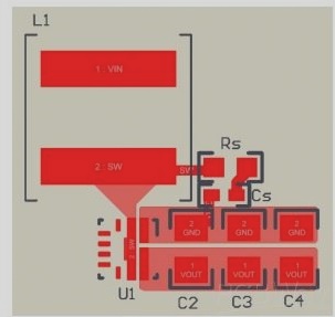
Designing a High-Quality PCB for Boost Converters
While copying the boost converter’s reference design may seem like an easy solution, it may not always be compatible with the specific system board you’re working with. To optimize PCB layout for a boost converter, consider the following design steps:
- Proper placement and routing of the output capacitor: The output capacitor should be positioned close to the IC, with a short, wide trace connecting the capacitor to the transistor. This minimizes current losses and improves efficiency. The transistor should also be placed near the IC to ensure effective current flow, as the current through the external transistor is pulsed.
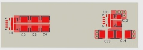
- Inductor placement: The inductor should be positioned near the IC to minimize electromagnetic interference (EMI). The copper area around the node should be designed to handle high current while minimizing the footprint. Sensitive signal nodes should be isolated to prevent noise interference.
- Input capacitor positioning: The input capacitor helps regulate current flow. Its ground node should be placed near the IC’s ground pin to minimize loop inductance. The boost converter’s power ground consists of the input transistor ground, the external transistor ground, and the IC’s ground pin. To ensure high efficiency, a larger copper area can be used on the input node to dissipate heat, especially when VIN voltage is stable. The snubber circuit, though crucial in some cases, won’t be discussed in detail here as it is not used in most applications.
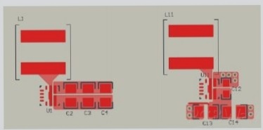
- Digital and small-signal modules: Resistors and capacitors for small-signal analog components are important for controlling noise. High-impedance signals, such as those at the input pins, can pick up switch noise if traces are too close. To reduce this effect, keep noise-sensitive signals away from high-power components.
- Signal grounding: Small-signal analog components should have their ground nodes connected to a dedicated Signal Ground, which is then connected to the Power Ground at a single point. This helps prevent noise from coupling into the control circuitry, ensuring stable operation and accurate voltage regulation. Sensor connections are typically grounded to the logic circuits’ ground node, which can be connected to the Power Ground if necessary, ensuring that the logic circuits remain unaffected by voltage noise.
Wellcircuits offers a wide range of PCB services, including Aluminum PCBs, Rigid PCBs, Metal Core PCBs, Flexible PCBs, and more.
If you are interested in receiving a PCB layout for a boost converter, feel free to contact us at contact@wellcircuits.com.
If you have any questions about PCB design and assembly, please don’t hesitate to reach out to us at info@wellcircuits.com.