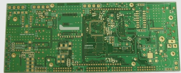
Advanced Manufacturing Technology:
1. Build-Up Method for High-Density Interlayer Connection (HDI) PCB Technology The build-up method is a new technology that cooperates with the manufacture of blind hole boards. The method is to first process the inner layer according to the ordinary multi-layer board processing method, and then superimpose the upper and lower layers, two or more layers, we call it build-up layer or SBU layer. The SBU layer and its adjacent layers are connected by micro through holes (ie blind holes). To truly master this technique, you must first master the following techniques:
A. Laser Drilling Technology Although a laser drilling machine can be used to drill blind holes of 2mil-8mil, the laser drilling technology is much more complicated than ordinary mechanical drilling. When the S-reverse material is different, the thickness of the board is different, and the aperture is different, the required laser energy is different. Therefore, we must go through systematic trials and tests to find out the drilling parameters suitable for various boards, so as to ensure the drilling quality.
B. Micro-Through Hole Plating Technology HDI boards usually contain buried holes and blind holes. The diameter of the buried holes is about 0.3mm, and the diameter of the blind holes is 0.1-0.15mm. In ordinary PCBs, the minimum through-hole diameter is 0.5mm, and there are no blind holes. Therefore, to produce HDI boards, blind hole plating is a problem that must be solved. The positive and negative pulse electroplating power supply is used, and the design of the electroplating line is improved, so that the thickness ratio of the coating layer in the blind hole and the coating layer on the surface can be close to or higher than 1:1, and the HDI board has good reliability.

