Understanding Signal Integrity in High-Speed PCB Design
Introduction
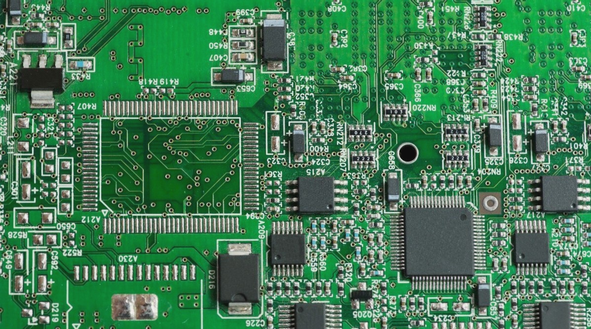
Printed circuit boards (PCBs) play a crucial role in supporting circuit components and electronic devices in various products. The quality of PCB design significantly influences the reliability and compatibility of embedded systems. In the past, low-speed circuit boards operated at around 10 MHz, with simple and transparent interconnect lines. However, with the rise of high-frequency circuits in modern embedded systems, signal integrity has become a critical concern.

Signal Integrity
Signal integrity is essential for controlling waveform distortion, meeting timing requirements, and ensuring stable signal transmission, especially in high-speed digital circuits. External interference and spectral dispersion can degrade signal integrity, leading to challenges in achieving expected signal destinations. Factors such as jitter, delay, reflections, crosstalk, and noise impact signal integrity, requiring a comprehensive understanding of the signal environment.
Delay
Signal delay along PCB traces affects system timing, influenced by trace length and dielectric constant. Excessive phase differences due to signal delay can result in erroneous signals in high-speed digital systems.
Reflection
Reflection occurs when signal delay exceeds transition times, causing impedance mismatches and signal power reflections. Trace geometry, terminations, and connector transitions contribute to reflections in PCB designs.
Crosstalk
Crosstalk, induced by mutual inductance and capacitance between signal lines, can affect signal quality. Managing crosstalk involves optimizing PCB layer parameters, signal line spacing, and termination strategies.
Overshoot and Undershoot
Overshoot and undershoot refer to signal deviations beyond voltage thresholds, impacting circuit reliability and potentially causing data errors.
Oscillation and Ground Bounce Noise
Oscillations from under-damped signal transitions and ground bounce noise from transient current surges can affect circuit behavior and reliability, especially under load conditions.
Analysis of PCB Transmission Channel Electrical Characteristics
In multi-layer PCBs, transmission lines span multiple layers interconnected via vias. At high frequencies, their electrical characteristics, such as impedance variations and parasitic effects, have a significant impact on signal quality.
Transmission Line Electrical Characteristics in High-Speed PCBs
High-speed PCB design requires the management of signal paths with varying lengths, incorporating distributed parameters like resistance, capacitance, and inductance that affect signal propagation and integrity.
Via Electrical Characteristics in High-Speed PCBs
Vias, crucial for inter-layer connectivity, introduce parasitic capacitance and inductance that affect signal rise times and power supply effectiveness in high-speed PCBs.
Impact of Transmission Line Corners on Signal Integrity
Changes in trace width at PCB corners can alter characteristic impedance, leading to signal reflections that degrade signal integrity, especially at higher frequencies.
Wiring Techniques to Improve Signal Integrity
To mitigate signal integrity issues, it is essential to maintain uniform transmission line characteristics, minimize impedance changes, optimize trace layout, and reduce parasitic effects such as via and corner placement.
Conclusion
Signal integrity plays a crucial role in embedded systems PCB design, influencing overall success. Effective management through strategic layout and wiring techniques enhances reliability, reduces signal integrity-related losses, and ensures robust performance in high-frequency environments.