PCB Multilayer Board Manufacturing Technology
Introduction to Advanced Techniques
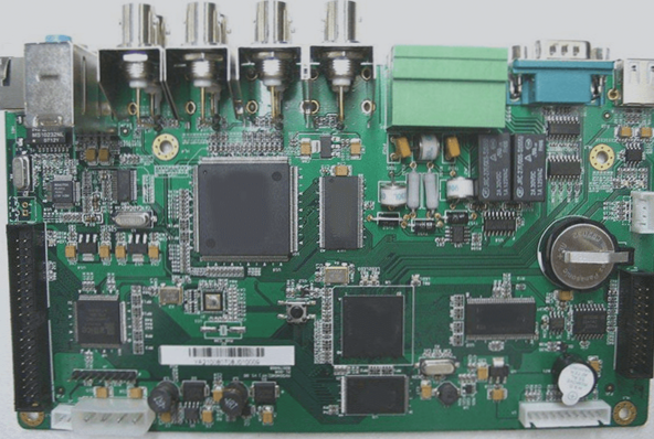
When it comes to PCB multilayer board manufacturing, various cutting-edge techniques are employed to ensure precision and reliability. From High-Density Interconnection (HDI) printed boards to the Thermosetting Ink Layering Method (TCD), the industry is constantly evolving to meet the demands of modern electronics.
1. High-Density Interconnection (HDI) PCB Circuit Board Technology Using the Build-Up Method
The build-up method revolutionizes PCB manufacturing by incorporating blind holes and stacked layers. This innovative approach involves intricate processes like laser drilling, micro-via plating, and fine line production to achieve high-density interconnections.
- Laser Drilling Technology: Laser drilling is a sophisticated technique essential for creating tiny holes with precision. Adjusting laser energy levels based on material and hole specifications is crucial for optimal results.
- Micro-via Plating Technology: HDI boards with buried and blind holes require specialized plating methods to ensure reliability. By utilizing advanced electroplating techniques, the thickness ratio of plating layers can be maintained for enhanced performance.
- Fine Line Production Technology: Achieving narrow line widths and spacings is a hallmark of high-density circuit boards. Advanced production lines and exposure technologies enable the creation of ultra-fine lines, pushing the boundaries of PCB design.
Recent Developments in PCB Manufacturing
Recent advancements in PCB manufacturing include the integration of high-end special materials, such as advanced substrates and conductive inks, to enhance performance and durability. Additionally, plating and filling blind hole technology (Via Filling) has gained prominence for its ability to improve signal integrity and reliability in multilayer boards.
Looking Ahead
As technology continues to advance, PCB manufacturers are exploring new methods to meet the growing demands of the electronics industry. From miniaturization to enhanced functionality, the future of PCB multilayer board manufacturing holds exciting possibilities.