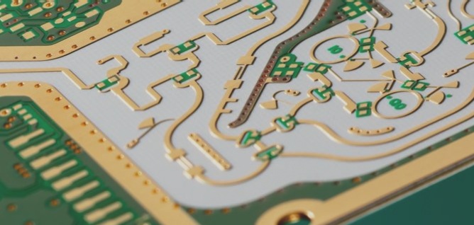
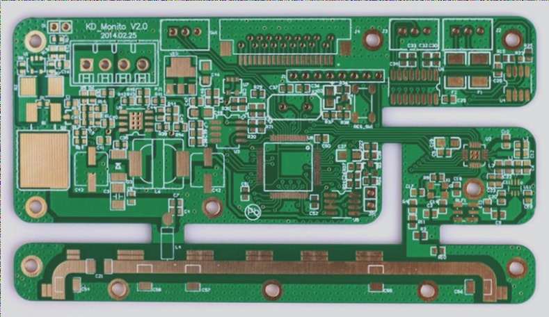
The TCD process mainly encompasses the following technical aspects:
A. Plug Hole Technology: Before applying thermosetting ink through screen printing, it’s imperative to fill the inner through holes with plugging oil. Failing to plug the holes beforehand may result in depressions around the orifices post-printing, accompanied by air bubbles within the hole. Surface irregularities directly impede circuit production, while gas expansion within the hole during heating renders the PCB unable to pass the thermal shock test. This underscores the critical importance of hole plugging quality, necessitating the assurance of 100% hole fill for each board.
B. Screen Printing Technology: In TCD technology, screen printing quality stands as a pivotal factor. Addressing concerns such as controlling ink thickness post-curing to meet customer specifications, ensuring ink flatness, managing ink expansion and contraction post-baking, controlling board surface warpage, etc., is imperative.
C. Surface Roughening Technology of Ink Layer: Adequate surface roughening of the ink layer is essential to establish a robust bond between the ink layer and the copper layer post-PTH. Following circuit formation on the copper layer, wire tension should exceed ≥1.0kg/cm.
D. Electroless Copper Sinking Technology: Electroless copper sinking on the ink layer’s surface deviates significantly from hole metallization in conventional boards. Unlike ordinary boards’ hole metallization (PTH), which deposits copper to interconnect various layers passing through the hole, non-electrostatic copper deposition on the ink surface necessitates uniform distribution across positive blind holes and surfaces within the through hole. After electroplating thickening, the line tension between ink layers must meet standard requirements, exhibiting no delamination post-thermal shock (260℃ for 20s). Achieving this mandates a slow initial reaction rate during electroless copper sinking to minimize internal stress, as failure to do so could lead to delamination following thermal shock.