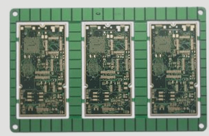
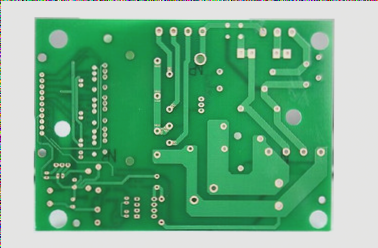
1. Depending on the function and design of electronic devices, printed circuit boards (PCBs) can be categorized into single-sided, double-sided, and multi-layer boards based on the number of circuit layers.
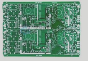
2. Multi-layer boards can have over a dozen layers. The advent of High Density Interconnect (HDI) PCBs has enabled mobile phones, ultra-thin laptops, tablets, digital cameras, automotive electronics, and other electronic products to optimize motherboard designs, achieving goals of reduced size, weight, and thickness.
3. More importantly, this advancement allows for additional internal space for batteries, thereby extending device battery life.
4. The primary distinction between HDI technology and traditional printed circuit boards lies in the method of hole formation. While traditional PCBs employ mechanical drilling, HDI boards utilize non-mechanical methods such as laser drilling.
5. HDI boards are produced using the build-up method. Typically, HDI boards utilize primary build-up, whereas high-end HDI boards may employ secondary or more advanced build-up techniques, incorporating electroplating to fill through-holes and stacked vias simultaneously.
6. Additionally, advanced PCB technologies like shot direct punching are applied.
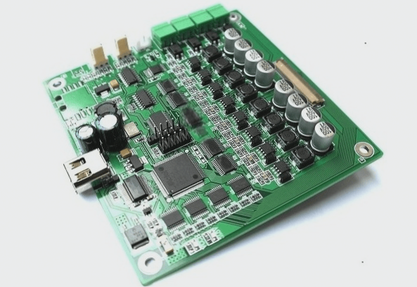
7. Mobile phone manufacturers increasingly favor high-density interconnection boards.

1. The utilization of high-density interconnect (HDI) boards has become extremely widespread. For instance, modern smartphones primarily utilize HDI boards, including Any Layer HDI. The distinction between the HDI process of Any Layer HDI and traditional HDI lies in the former’s ability to bypass the intermediate substrate, allowing for a thinner product design. Typically, transitioning from first-order HDI to Any Layer HDI can result in a volume reduction of approximately 40%.
2. Both Apple and non-Apple products heavily incorporate Any Layer HDI boards, primarily to achieve lighter and thinner designs while maximizing internal space for batteries, thereby enhancing battery life.
3. Recognizing significant business opportunities, automation and PCB equipment manufacturers are advancing their technologies. Notably, the direct imaging exposure machine technology developed by Chuanbao Technology in the U.S. has been transferred to Taiwan for local production. Chuanbao collaborated with Maskless Lithography in the U.S. to secure technology transfer and patent rights, facilitating this introduction.
4. In terms of producing high-end thin PCBs and circuits, the trend is moving away from film exposure toward direct imaging. Additionally, Guangyun Machinery is entering the high-end Any Layer HDI process PCB equipment market through project initiatives.
5. The introduction of substrate-like HDI technology aligns with the evolution of System in Package (SiP) technology, where line spacing and width are advancing towards finer pitches, specifically requiring dimensions below 35 microns. This represents a significant shift from standard HDI boards. Due to the drastic reduction in these dimensions, traditional HDI processes are insufficient, necessitating a semiconductor IC substrate production approach for HDI-like substrates.
6. The realization of 3D-printed multilayer boards is a notable development. PCB manufacturing technology is rapidly evolving; using 3D machines to create simple PCBs is increasingly common. At the SolidWorks World 2016 conference, Israel’s Nano Dimension unveiled the DragonFly 2020, the first 3D printer capable of producing professional multilayer circuit boards using specialized nano-level conductive materials.
7. Simon Fried, co-founder of Nano Dimension, emphasized that this machine is the world’s first capable of printing multilayer circuit boards, supporting through-hole designs. The printed boards can also be soldered with electronic components like traditional boards, enabling the creation of up to 10 layers within a few hours.
8. Fried highlighted that the critical factor in printing multilayer circuit boards is Nano Dimension’s proprietary AgCite silver conductive material, which can produce extremely fine ink droplets for both flat and three-dimensional electronic circuits. The DragonFly 2020 utilizes inkjet technology with dual nozzles, layering conductive and insulating materials to construct multilayer boards featuring both planar and 3D circuits. However, the technology currently supports a minimum line width of 90 microns, and the high cost of silver conductive materials limits its application to prototyping and low-volume production.
9. The complexity of HDI boards presents unique verification challenges. Unlike traditional multilayer boards, the testing requirements for HDI boards are distinct. As HDI boards become increasingly thinner and as lead-free technology evolves, the challenges related to heat resistance are intensifying, raising reliability standards.
10. Heat resistance refers to a PCB’s capacity to endure thermo-mechanical stress during soldering. It is crucial to note that the layer structure of HDI boards differs from standard multilayer through-hole boards, leading to unique heat resistance issues. The primary defects in first-order HDI boards include board bursting and delamination, particularly in areas above dense buried vias and below large copper surfaces—key focus points for HDI testing.
11. Overall, as circuits on multilayer boards grow more complex and substrate sizes shrink, manufacturing processes are becoming increasingly intricate, heightening the difficulty of final product verification. To ensure quality and avoid defects, it is essential to utilize advanced testing equipment for comprehensive electrical evaluations.
—
If you need further adjustments, feel free to ask!
2. Multi-layer boards can have over a dozen layers. The advent of High Density Interconnect (HDI) PCBs has enabled mobile phones, ultra-thin laptops, tablets, digital cameras, automotive electronics, and other electronic products to optimize motherboard designs, achieving goals of reduced size, weight, and thickness.
3. More importantly, this advancement allows for additional internal space for batteries, thereby extending device battery life.
4. The primary distinction between HDI technology and traditional printed circuit boards lies in the method of hole formation. While traditional PCBs employ mechanical drilling, HDI boards utilize non-mechanical methods such as laser drilling.
5. HDI boards are produced using the build-up method. Typically, HDI boards utilize primary build-up, whereas high-end HDI boards may employ secondary or more advanced build-up techniques, incorporating electroplating to fill through-holes and stacked vias simultaneously.
6. Additionally, advanced PCB technologies like shot direct punching are applied.
7. Mobile phone manufacturers increasingly favor high-density interconnection boards.
1. The utilization of high-density interconnect (HDI) boards has become extremely widespread. For instance, modern smartphones primarily utilize HDI boards, including Any Layer HDI. The distinction between the HDI process of Any Layer HDI and traditional HDI lies in the former’s ability to bypass the intermediate substrate, allowing for a thinner product design. Typically, transitioning from first-order HDI to Any Layer HDI can result in a volume reduction of approximately 40%.
2. Both Apple and non-Apple products heavily incorporate Any Layer HDI boards, primarily to achieve lighter and thinner designs while maximizing internal space for batteries, thereby enhancing battery life.
3. Recognizing significant business opportunities, automation and PCB equipment manufacturers are advancing their technologies. Notably, the direct imaging exposure machine technology developed by Chuanbao Technology in the U.S. has been transferred to Taiwan for local production. Chuanbao collaborated with Maskless Lithography in the U.S. to secure technology transfer and patent rights, facilitating this introduction.
4. In terms of producing high-end thin PCBs and circuits, the trend is moving away from film exposure toward direct imaging. Additionally, Guangyun Machinery is entering the high-end Any Layer HDI process PCB equipment market through project initiatives.
5. The introduction of substrate-like HDI technology aligns with the evolution of System in Package (SiP) technology, where line spacing and width are advancing towards finer pitches, specifically requiring dimensions below 35 microns. This represents a significant shift from standard HDI boards. Due to the drastic reduction in these dimensions, traditional HDI processes are insufficient, necessitating a semiconductor IC substrate production approach for HDI-like substrates.
6. The realization of 3D-printed multilayer boards is a notable development. PCB manufacturing technology is rapidly evolving; using 3D machines to create simple PCBs is increasingly common. At the SolidWorks World 2016 conference, Israel’s Nano Dimension unveiled the DragonFly 2020, the first 3D printer capable of producing professional multilayer circuit boards using specialized nano-level conductive materials.
7. Simon Fried, co-founder of Nano Dimension, emphasized that this machine is the world’s first capable of printing multilayer circuit boards, supporting through-hole designs. The printed boards can also be soldered with electronic components like traditional boards, enabling the creation of up to 10 layers within a few hours.
8. Fried highlighted that the critical factor in printing multilayer circuit boards is Nano Dimension’s proprietary AgCite silver conductive material, which can produce extremely fine ink droplets for both flat and three-dimensional electronic circuits. The DragonFly 2020 utilizes inkjet technology with dual nozzles, layering conductive and insulating materials to construct multilayer boards featuring both planar and 3D circuits. However, the technology currently supports a minimum line width of 90 microns, and the high cost of silver conductive materials limits its application to prototyping and low-volume production.
9. The complexity of HDI boards presents unique verification challenges. Unlike traditional multilayer boards, the testing requirements for HDI boards are distinct. As HDI boards become increasingly thinner and as lead-free technology evolves, the challenges related to heat resistance are intensifying, raising reliability standards.
10. Heat resistance refers to a PCB’s capacity to endure thermo-mechanical stress during soldering. It is crucial to note that the layer structure of HDI boards differs from standard multilayer through-hole boards, leading to unique heat resistance issues. The primary defects in first-order HDI boards include board bursting and delamination, particularly in areas above dense buried vias and below large copper surfaces—key focus points for HDI testing.
11. Overall, as circuits on multilayer boards grow more complex and substrate sizes shrink, manufacturing processes are becoming increasingly intricate, heightening the difficulty of final product verification. To ensure quality and avoid defects, it is essential to utilize advanced testing equipment for comprehensive electrical evaluations.
—
If you need further adjustments, feel free to ask!