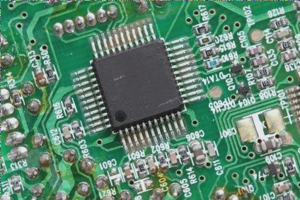
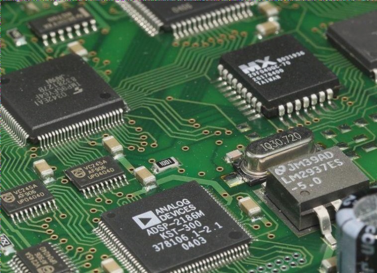
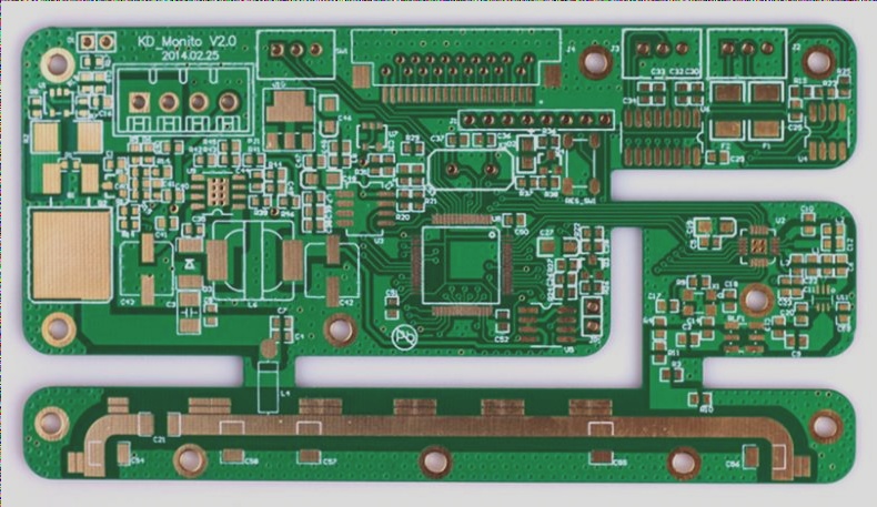
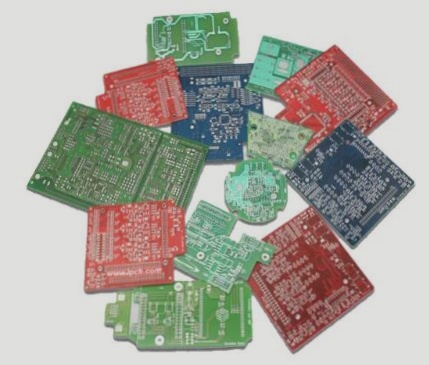
HDI (High-Density Interconnector) PCBs refer to printed circuit boards (PCBs) with a higher number of interconnections per unit area compared to traditional PCBs, characterized by their high layer count, fine line widths, and spaces, enabling improved electrical performance and miniaturization.
1. **Reduced Size:** HDI rigid boards facilitate the miniaturization of electronic devices, enhancing their compactness and portability.
2. **Enhanced Electrical Performance:** The increased number of interconnections in HDI rigid boards enables more efficient signal routing, reducing signal loss and enhancing signal integrity.
3. **Cost Savings:** HDI rigid boards can be more cost-effective than traditional PCBs due to their smaller size and weight.
4. **Increased Manufacturing Flexibility:** HDI rigid boards can be manufactured using various techniques, such as multi-layer lamination and through-hole plating, providing manufacturers with greater flexibility in PCB design and production.
HDI (High-Density Interconnector) printed circuit boards have garnered significant attention in the electronics industry for their outstanding performance and compact design, meeting the growing demand for high performance and miniaturization.
One of the primary reasons why HDI rigid PCBs have gained popularity is the increased density they offer. By stacking multiple layers using microvia technology and blind vias, manufacturers can achieve higher component density, thereby reducing the overall size of the printed circuit board. This miniaturization enables designers to create more compact and space-efficient electronic devices.
Another key advantage of HDI rigid boards is their capability to integrate multiple layers, which enhances the complexity of PCB designs. Conventional PCB technologies typically limit manufacturers to five or six layers, whereas HDI rigid boards can incorporate up to 24 layers. This capability facilitates the integration of more complex circuitry, ultimately reducing the size and weight of electronic devices.
Signal integrity is a critical concern for designers working on high-speed electronic devices. HDI rigid boards offer significant improvements in signal integrity due to the use of microvias and blind vias. These technologies enable shorter signal paths, resulting in reduced signal loss and higher data transfer speeds. Additionally, the controlled impedance provided by HDI rigid PCBs ensures consistent signal propagation, thereby enhancing overall performance.
1. HDI rigid boards are renowned for their enhanced mechanical durability. The utilization of microvias and blind vias in HDI rigid PCBs fortifies structural integrity, averting delamination and cracking. Furthermore, the downsized components and augmented layer count foster a more resilient design. This durability ensures an extended lifespan and dependable performance, even in demanding applications.
2. Contrary to common belief, HDI rigid PCBs can yield cost savings for manufacturers. The heightened density and enhanced signal integrity permit the utilization of smaller components, thereby curtailing overall material costs and assembly intricacies. Moreover, the abbreviated signal paths and diminished board sizes lead to decreased power consumption, further enhancing the cost-effectiveness of HDI rigid boards.
1. In conclusion, HDI rigid boards have emerged as a superior development trend in the printed circuit board industry.
2. The ability to provide higher density, multilayer integration, improved signal integrity, enhanced mechanical durability, and cost reduction make them an ideal choice for high-performance and compact electronic devices.
3. As technology continues to advance, we can expect further advancements in HDI rigid PCB technology to cater to the growing requirements of electronic systems.