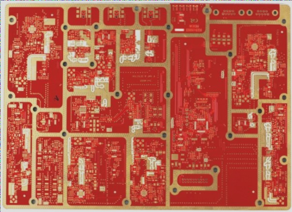
Multi-layer circuit boards are commonly used in high-speed PCB design. These boards are created by laminating and bonding several etched single-sided or double-sided boards together. When compared to single- and double-layer circuit boards, multi-layer circuit boards offer numerous advantages, particularly in small-volume electronic products. Let’s explore the key benefits of multi-layer circuit boards.
1. Multi-layer circuit boards offer high assembly density and compact size. As electronic devices continue to shrink, there are increasing demands on PCB electrical performance, which in turn drives the growing need for multi-layer circuit boards.
2. The use of multi-layer circuit boards simplifies the routing process, significantly reduces the length of the traces, and shortens the connections between electronic components. This, in turn, enhances the speed of signal transmission.
Here is the revised version of the article with slight rephrasing, maintaining the original meaning, clarity, and technical accuracy:
3. For high-frequency circuits, adding a ground layer helps to establish a consistent low impedance path to ground. This significantly reduces circuit impedance and improves shielding effectiveness.
4. For electronic products with high heat dissipation requirements, multilayer PCBs can incorporate a metal core heat dissipation layer, which effectively addresses the needs for functions like shielding and thermal management.
In terms of performance, multi-layer circuit boards outperform single- and double-layer boards. However, the more layers a board has, the higher the production cost, the longer the processing time, and the more complex the quality inspection process becomes. Despite the higher cost of multilayer boards when compared to single- and double-layer boards over the same area, the cost difference becomes less significant when considering the noise reduction benefits. With advancements in technology, PCB boards with over 100 layers are now being used in high-precision aerospace instruments and medical equipment.
The most common multilayer PCBs are four-layer or six-layer boards, and these are widely used in everyday products such as computers. The key difference between a four-layer and a six-layer board lies in the additional internal signal layers between the ground and power layers in the six-layer design. This makes the six-layer board thicker than the four-layer version. Single- and double-layer boards are easy to distinguish visually; by holding the board up to the light, you’ll see that apart from the wiring on both sides, the rest of the board is transparent. However, distinguishing between a four-layer and a six-layer board is not as straightforward unless there are specific markings on the board.
In general, multilayer circuit boards are widely used in electronics due to their design flexibility, economic advantages, stable electrical performance, and reliability.
Lastly, let’s discuss PCB layout. First, consider the size of the PCB. A larger PCB reduces the system’s ability to resist interference and increases costs due to more traces, while a smaller PCB can cause issues with heat dissipation and signal interference. Second, pay attention to the placement of special components, such as clock components. Clock traces should ideally not be grounded or run along critical signal paths to avoid interference. Finally, design the PCB layout based on the overall circuit functions. In component placement, related components should be positioned as close as possible to improve the anti-interference performance.
If you have any PCB manufacturing needs, please do not hesitate to contact me.Contact me