The Importance of PCB Mirror Boards in PCBA Manufacturing
The typical PCB structure positions the CS and SS layers on the top and bottom sides of the board, respectively. However, in some cases, a PCB Mirror Board is required to allow soldering of components on both SS layers and separate PCBs on the CS layers.
Types of PCB Mirror Boards
- Different Side Mirror Board: One side of one board appears mirrored on the opposite side of another board.
- Same Side Mirror Board.
PCBA manufacturers require PCB Mirror Board designs for two main reasons and benefits:
1. Maximizing SMT Line Efficiency
The efficiency of an SMT line is crucial in PCBA manufacturing. By utilizing PCB Mirror Boards, manufacturers can fully leverage the advantages of SMT long lines to achieve higher efficiency. Panelization plays a key role in enhancing the utilization of pick-and-place machines, allowing for continuous operation without downtime.
Enhanced Efficiency with Panelization
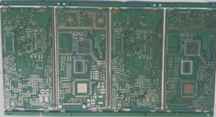
Arranging boards in a positive and negative inverted Yin-Yang pattern on panels enables SMT long lines to operate at full capacity. This strategy minimizes idle time and maximizes production capacity, ultimately improving overall efficiency in PCBA manufacturing.
2. Space Optimization and Cost Reduction
PCB Mirror Boards help save space wasted by PCB bare boards, leading to increased Panelization efficiency and reduced costs. By combining multiple PCBs into a single board layout, manufacturers can optimize production, enhance board efficiency, and achieve cost savings.


