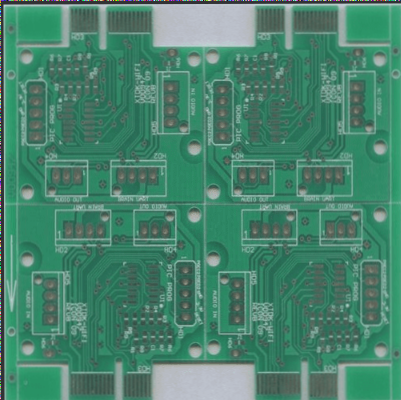
The electronics and computing industries have seen a lot of advancements over the years, thanks to the advancements in the PCB industry. IC is one of the most important components of a PCB, and it has also advanced a lot with the technological improvements in IC substrate. So, what is IC substrate and how does it brings several benefits to the IC? Here we will discuss everything you need to know about IC Substrate.
What is IC Substrate?
An IC is an integrated chip with tiny components inside it. Leaving those components bare is not feasible, so it is necessary to pack those components. Here we use the IC Substrate as a baseboard for packing the components inside an IC. Here the Substrate also provides the connection point for connecting the circuit board with the semiconductor chip.
So, the IC Substrate serves to provide structural support for the IC chip as well as providing thermal protection. IC Substrate is important in connecting the PCB with the internal chip with the pins passing through it.
Different types of IC Substrate according to packing
There are different types of IC depending on their structure and functionality. So, the IC Substrate there is also different. Below are the details about IC Substrate for different types of ICs.
BGA
The BGA Chips have a BGA IC Substrate that focuses on electrical performance and thermal dissipation. It is good for heat dissipation because of the increased number of pins. However, the BGA IC Substrate is only good for cases with a connection pin count above 300.
CSP
The CSP IC Substrate is a good option for the smaller chip size because of the lightweight single chip with fewer connection pins. This type of IC Substrate is a good option for telecommunication ICs as well as memory ICs. One main requirement for the CSP IC Substrate is having a smaller number of pins.
FC
The Flip Chip ICs use FC IC Substrate, vital for maintaining the best signal quality while providing good thermal dissipation. FC IC Substrate provides low circuit loss to maintain the low signal interference.
MCM
The MCM IC Substrate is used in multiple chip modules where the main features are thinness, small size, and lightweight. While it works amazingly in this category, it is not good in maintaining low signal interference, thermal dissipation, and critical things. It is because the IC Substrate packs a lot of chips in a single housing.
Different types of IC Substrate according to material
IC substrate may differ depending on the material characteristics used. Below are the 3 different types.
Rigid
It is made with ABF resin, Epoxy resin, or BT risen. It has a thermal expansion coefficient of approximately up to 17ppm/°C.
Flex
Flex IC Substrate is made with PI or PE resin. It has a thermal expansion coefficient of approximately 27ppm/°C.
Ceramic
Ceramic IC Substrate has ceramic materials like Silicon carbide, Aluminum Oxide, or Aluminum nitride. It has a thermal expansion coefficient of approximately 8ppm/°C.

Different types of IC Substrate according to bonding
The IC Substrate is also available with different bonding types. The 3 types of bonding technologies used are:
- TAB(Tape Automated Bonding)
- FC Bonding
- Wire Bonding
With 4 different packing types, 3 different bonding types, and 3 different materials for making the IC Substrate, it is now possible to create an IC substrate for any application according to its requirements. It is extremely important to use the IC Substrate of the right type according to its requirements, considering the role of the IC Substrate in the proper functionality and performance of the electronics.
What is the IC Substrate manufacturing process?
If you were looking for what is IC Substrate manufacturing process, then here we have all the steps that are a part of the process. Remember that this IC Substrate is the primary connection between the IC and the PCB with solder points. Below are all the steps we need to follow to manufacture the IC Substrate.
- Circuit designing
The first part of the process here is designing. It is important to meet the dimensions of the IC as well as the soldering points and their positioning. During the designing phase, professionals consider all of the following things:
- Material composition
- Applicable substrate types
- Rigid vs. Tape substrates
- Substrates for assisting metal conductors
So, the professionals will design the IC Substrate in the first step of its manufacturing.
- Copper plating
The next step includes copper plating after patterning. Copper plating technology and patterning technology are used here to meet the needs of circuit connections. It is necessary to have a fine and equal layer of the copper plate all around. Thus, fine-line fabrication equipment and techniques are used here.
- Solder masking
Solder masking is the next step, and it takes copper patterning and copper plating to the next step. The solder mase includes solder hole filling and solder mask printing equipment. Keeping less than 10-micrometer of height difference in the Substrate and the solder pad is necessary. So fine solder masking equipment technology is used.
- Finishing
Surface finishing is also important to ensure that the IC Substrate gets an even surface with the recommended thinness and surface finish. Here ENIG and ENEPIG surface finishes are usually utilized for all IC Substrates.
- Inspection and testing
The manufacturing process is complete, and now final inspection and testing are left. The IC Substrate goes through reliability, quality, and performance testing using different technologies and equipment for testing. Remember that this inspection and testing is different from the Standard PCB testing.
This process may not be that straightforward, but the steps may make it easier for you to comprehend. With these 5 steps, the process of IC Substrate is complete.
What are the different technologies that are used in IC Substrate manufacturing?
What is IC Substrate manufacturing? It is a process that is complete after using many different technologies during different stages of the process. Some of those technologies include:
- Direct imaging
- UV Laser – Drilling
- Automated Optical Inspection
- Additive printing
- Automated Optical Shaping
These are the 5 main technologies used for the IC Substrate manufacturing process.
What are the features and benefits of IC Substrate?
An IC Substrate has several characteristics that make it beneficial for electronic PCBs. Below are the details of some of the features and benefits we can avail of because of IC Substrate.
Small size saves a lot of space.
The first benefit here is that the whole circuit is miniaturized. When a circuit is made in the form of an integrated circuit chip, it can get extremely small. That saves a lot of space whether we consider packaging or PCB real estate. Thus, it also helps in making the size of electronics smaller.
Easier debugging
IC Substrate makes debugging easier. Instead of dealing with an open circuit with wires and pins, an IC has fewer pins thanks to good packing with proper pins using the IC Substrate. The schematic of IC also helps, and the overall debugging process becomes easier.
Cheaper
Manufacturing, application, and replacement are easier with IC substrate than with open circuits. It is because there is much more to do when dealing with open circuits and their discrete components. Packing the whole circuit as an integrated circuit with the help of IC Substrate brings cost savings.
Reliable
Reliability increases considering the integrated circuit substrate usage. The circuit itself is good in terms of performance and heat dissipation. The soldering joints inside the circuit and on the PCB are also stronger with the usage of IC Substrate. So, the circuit can withstand any jerks without any issues.
Less complex
IC Substrate makes the overall circuit on a PCB less complex. It is because most of the complex parts of the circuit are packed within the IC with the help of the IC Substrate. So, there are fewer bare wires and terminals to get solder joints. Thus, IC Substrate decreases the overall complexity of any PCB.
Efficient
IC substrate lets pack circuit inside a small package that enhances the efficiency of the circuit. These consume less power and maintain better low signal disturbance. Additionally, the chances of failure and errors are lesser than in regular circuits.
Modern-day applications of the IC Substrate and the PCBs that use them.
Today we have devices and appliances that are becoming thinner and lightweight while providing better performance and functionality. These devices hold such capabilities only because of the IC Substrate and the compatible PCBs. The IC Substrate helps make the whole thing:
- Thinner
- More powerful
- More efficient
- Bring advanced features
It is the reason the most common applications of IC Substrate are Smartphones, Laptops, Computer parts, Telecommunication, and medical care, where small devices need to perform well.
Conclusion
It was all about what is IC Substrate. We hope all your queries regarding the types, benefits, and manufacturing of the IC Substrate are clear now. Now selecting the right type of IC and IC Substrate will be easier and better for you considering the technicalities that affect the performance.


