The Importance of Amplifier Circuit Design
An amplifier circuit is crucial for boosting audio signals from various sources like microphones or audio devices to drive speakers or radios effectively. Whether it’s an audio amplifier or a Wi-Fi amplifier, the circuit layout significantly impacts signal quality. Poor design choices during the PCB phase can lead to issues like leakage currents, voltage drops, or parasitic capacitance, affecting overall performance.
Enhancing Amplifier Performance with PCB Layout
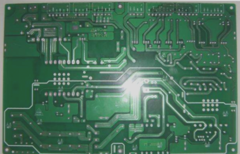
The PCB layout for amplifiers involves designing copper traces and components to amplify signals efficiently. Amplifier PCBs play a vital role in converting analog signals to digital, ensuring signal amplitude, frequency stability, and high voltage output. They are essential for driving loudspeakers and maintaining proper signal conditioning between the circuit and the receiver.

Optimizing PCB Layout for Amplifiers
When designing the PCB layout for an amplifier, consider the Dynamic Modules Selection Guide for Class-D Audio Amplifiers to choose the best components. Utilize multi-layer PCBs with epoxy-filled layers for improved performance. Here are some guidelines to follow:
1. Power Plane Design:
- Ensure thick power planes to meet current demands.
- Route power planes in a star configuration to minimize interference.
- Place bypass capacitors close to IC pins for stable power supply.
2. Ground Connections:
- Directly connect ground pins to the ground plane to avoid loops.
- Tie all ground pins closely to the ground plane for proper current return.
3. Capacitor Placement:
- Position capacitors near associated pins to reduce parasitic inductance.
- Minimize resistance between components and capacitors for better performance.
4. Signal Switching Considerations:
- Route high-frequency signals carefully to prevent interference.
- Avoid sharing signal layers unless adequately shielded.
5. Charge Pump Capacitor:
Consider the placement and usage of charge pump capacitors for efficient amplifier operation.
The Importance of PCB Layout for Amplifiers
When designing PCB layouts for amplifiers, it is crucial to consider various factors to ensure optimal performance and reliability.
1. Charge Pump Capacitor Placement:
It is essential to connect the charge pump capacitor with minimal parasitic inductance and resistance between the GREG/VREG and PVDD pins. Placing it close to the PVDD pin using a star connection and using thick traces can help reduce parasitic effects.
2. Class-D Output Signals Routing:
For Class-D output signals, routing should be done using at least two layers with a minimum trace width of 30 mils. To meet EMI specifications, output traces should have a width of 60 mils when routed to the speaker. Proper positioning of an EMI filter near the output pins is crucial to minimize signal degradation.
3. Digital Signal Routing:
Routing digital signals in a way that avoids interference with other signals is vital. Placing them away from switching nets can prevent noise and signal integrity issues. Proper isolation of digital signals is necessary to maintain signal quality and performance.
Advantages of Amplifier PCB Layout:
- Enhanced feedback loop and power quality for stable operation with minimal distortion.
- Efficient load driving capability by relaying half of a half-wave.
- Reduction in crossover distortion, resulting in cleaner output.
- Improved frequency response for greater reliability, especially in RF applications.
Disadvantages of Amplifier PCB Layout:
- Improper PCB trace installation may lead to frequent rework or component replacement.
- Potential damage to the PCB or structural failure if issues are not addressed promptly.
- Overheating of output devices due to inadequate heat management techniques.
- Increased current demands causing higher heat dissipation and component stress.
References:
For more information on amplifier PCB layout, you can visit https://www.venture-mfg.com/amplifier-pcb-layout/ and https://www.ti.com/lit/an/slaa896/slaa896.pdf. Feel free to reach out to us at info@wellcircuits.com for any inquiries regarding PCB and PCBA.