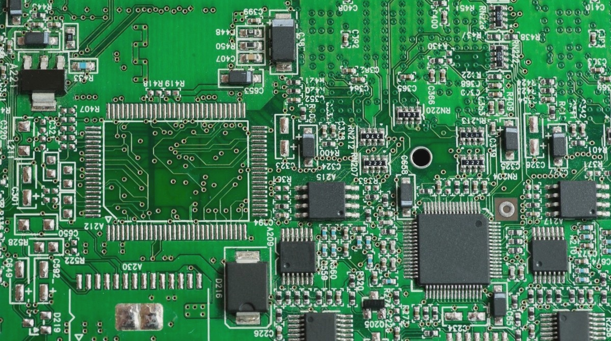
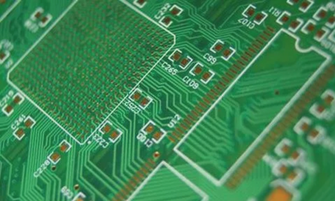
In order to ensure the quality of the printed circuit board (PCB) design, attention must be given to the wiring part of the PCB diagram during the design phase.
1. Component Layout
Reasonable arrangement of components forms the fundamental basis for creating a high-quality PCB layout. The requirements for component layout primarily encompass aspects such as installation, mechanical stress, thermal management, signal integrity, and aesthetics.
1.1. Installation
Installation involves meeting a set of basic requirements for seamlessly integrating the PCB into the chassis, enclosure, or slot within its intended application. This prevents issues like spatial interference and short circuits, ensuring that designated connectors align correctly with their corresponding positions on the chassis or enclosure. Detailed specifications are beyond the scope of this discussion.
1.2. Mechanical Strength
The circuit board must withstand various external forces and vibrations during installation and operation. Therefore, the PCB should have an appropriate shape, and the positions of various holes (such as screw holes and special-shaped holes) should be well-planned. Typically, the distance between a hole and the board edge should exceed the hole’s diameter to ensure adequate strength. Additionally, special attention must be given to prevent weak sections caused by irregular holes, especially for connectors extending directly from the device shell on the board, ensuring long-term reliability through secure fixation.
1.3. Thermal Management
For high-power devices that generate substantial heat, aside from ensuring proper heat dissipation, it’s crucial to position them appropriately. Particularly in sophisticated analog systems, the adverse thermal effects on delicate preamp circuits due to device-generated temperature fields must be carefully managed. Generally, high-power components should be modularized separately, with thermal isolation measures implemented between them and the signal processing circuit.
1.4. Signal Integrity
Signal interference is a critical consideration in PCB layout design. Key aspects include isolating weak signal circuits from strong ones, separating AC and DC components, and segregating high-frequency from low-frequency sections. Proper attention should also be paid to signal line direction and ground layout, as extensively covered in existing literature.
1.5. Aesthetic Considerations
Beyond orderly component placement, the elegance and smoothness of wiring are important. While amateurs may prioritize the former, especially when performance requirements are lenient, high-performance applications demand aesthetic wiring even within double-sided boards. Detailed discussions on wiring aesthetics will follow in the subsequent section.
2. Wiring Principles
Certain anti-jamming techniques not commonly found in literature are detailed below, primarily focusing on practical applications where double-sided panels remain prevalent.
2.1. Aesthetic Wiring
To minimize interference, avoid right angles during turns, favoring slashes or arcs for transitions. Wiring should be methodical and centralized, preventing signal cross-talk while easing inspection and modifications. For digital systems, segregate control signals like read, write, and clock from data and address lines, protecting them with dedicated ground lines. In extensive ground areas, maintain a balanced distance between ground “surfaces” and signal traces, maximizing proximity without risking short circuits or leaks. In low-current systems, keep ground and power lines close. For surface mount component systems, prioritize signal trace proximity to the top layer while dedicating the bottom layer predominantly to ground.
2.2. Ground Plane Layout
Despite extensive literature discussions, detailed guidance on practical PCB ground plane layout remains sparse. Emphasizing system reliability over prototyping, expansive ground “paving” in grid format enhances thermal performance and high-frequency conductivity. In double-sided designs, separating ground traces to accommodate signal routing compromises low ground resistance, necessitating strategic solutions to ensure smooth current flow. Techniques include maximizing surface mount component use to reclaim ground space and coordinating signal trace placement to prioritize critical board areas.
2.3. Power Line Routing and Filtering
Contrary to common belief, power line width does not universally demand thickness except for high-power scenarios, where wider lines accommodate currents upwards of 1A per second. Effective power noise mitigation hinges on filter capacitors; hence, investing in quality capacitors is essential for stringent power quality requirements. Capacitor types and their configurations vary by application—digital versus analog—and must be tailored to specific chip requirements, ensuring close proximity and direct connections for optimal filtering performance.
These refined principles ensure robust PCB design, aligning mechanical, thermal, signal integrity, and aesthetic considerations with practical application demands.