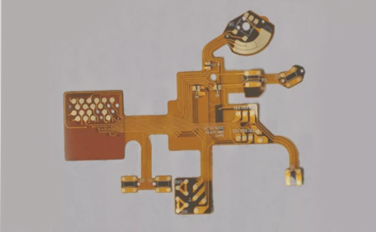
1. PCB, or Printed Circuit Board, serves not only as the support for electronic components but also as the carrier for their electrical connections. Before PCBs became prevalent, electronic components were connected through direct wiring. Today, this method is mostly confined to laboratory settings, with PCBs now dominating the electronics industry.
2. The history of PCB development dates back to the early 20th century. In 1936, Austrian inventor Paul Eisler first applied PCBs in radios, marking their practical debut. By 1943, the technology was widely adopted in military radios in the United States, and in 1948, it was officially recognized for commercial use. Consequently, PCBs began to see widespread use from the mid-1950s onward, entering a phase of rapid advancement.
3. As PCBs grow increasingly complex, designers often find themselves confused about the definition and purpose of each layer when using development tools. Hardware developers may inadvertently create production issues if they are unfamiliar with each layer’s function. To address this, we will use Altium Designer Summer 09 as an example to categorize and explain the purpose of each PCB layer.
Differences Between PCB Layers (Signal Layers)
Altium Designer can provide up to 32 signal layers, including the top layer (Top Layer), the bottom layer (Bottom Layer), and the middle layers (Mid-Layers). These layers can be interconnected through vias, blind vias, and buried vias.
**Explore the Mystery of Multilayer Circuit Boards**
1. **Top Layer**
Also known as the component layer, it is primarily used for placing components. In double-layer and multilayer boards, it can also be utilized for routing traces or copper.
2. **Bottom Layer**
Also referred to as the solder layer, it is mainly used for PCB wiring and soldering. In double-layer and multilayer boards, it can also accommodate components.
3. **Mid-Layers**
There can be up to 30 mid-layers, which are used for routing signal lines in a multilayer board. Power and ground lines are not included in these layers.
**Internal Power Planes**
Often abbreviated as internal planes, these are found only in multilayer boards. The number of PCB layers typically refers to the total count of both signal layers and internal power planes. Similar to signal layers, internal power planes can be connected to each other and to signal layers through vias, blind vias, and buried vias.
**Explore the Mystery of Multilayer Circuit Boards**
**Silkscreen Layers**
A PCB board can have up to 2 silkscreen layers: the top silkscreen layer (Top Overlay) and the bottom silkscreen layer (Bottom Overlay). Typically white, these layers are used for placing printed information such as component outlines, annotations, and various notes to assist in soldering and circuit inspection.
1. **Top Overlay**
Used to mark component outlines, labels, component values, models, and various annotations.
2. **Bottom Overlay**
Similar to the top silkscreen layer, this layer contains markings that correspond to those on the top layer, and if all markings are duplicated, the bottom silkscreen layer may be omitted.
**Mechanical Layers**
Mechanical layers are used to provide information about board manufacturing and assembly methods, such as PCB outline dimensions, size markings, data materials, via information, and assembly instructions. This information varies based on design company or PCB manufacturer requirements.
1. **Shape Layer**
Often used to draw the outline of the PCB, also known as the shape layer.
2. **Processing Requirement Form**
Used to specify PCB processing requirements, including dimensions, layers, and other specifications.
3. **Component Body Size Information**
Contains the body size information for most components in the ETM library, including three-dimensional models; this layer is not displayed by default for simplicity.
4. **Footprint Information**
Includes footprint data for most components in the ETM library, useful for estimating PCB size in the early project stages; this layer is not displayed by default and is colored black.
**Masking Layers**
Altium Designer provides two types of masking layers: solder mask layers and solder paste layers, each with a top and bottom layer.