### Introduction to the Types of Pads in PCB Boards and Their Application Advantages
1. **Circular Pads** – These are widely used in single-sided and double-sided printed circuit boards with regularly arranged components. If the board density allows, the pad can be larger to prevent detachment during soldering.
2. **Island-Shaped Pads** – These pads integrate the connection between the pad and the trace. They are commonly used in vertical and irregularly arranged installations, such as in tape recorders.
3. **Polygonal Pads** – These pads help distinguish between components with similar outer diameters but different apertures, facilitating easier processing and assembly.
4. **Oval Pads** – These pads provide sufficient area to enhance the anti-stripping capability and are frequently used in dual in-line packages.
5. **Open-Shaped Pads** – Designed to ensure that pad holes manually repaired after wave soldering are not sealed by solder.
6. **Square Pads** – More commonly used when the PCB components are large and few, and the printed wires are simple. Square pads are particularly useful for hand-made PCBs.

Plum Blossom Pad
1. The fixing hole should be non-metallized. During wave soldering, if the fixing hole is metallized, solder can block the hole during the reflow soldering process.
2. Fixing mounting holes arranged in a quincunx pattern are commonly used for GND networks, as PCB copper is typically used to lay out the GND network. After installing PCB shell components on quincunx holes, GND is effectively connected to the ground. Occasionally, the PCB shell also functions as shielding. However, some designs may not require connecting the mounting hole to the GND network.
3. Metal screw holes may become distorted, leading to grounding issues and unusual system anomalies. Plum blossom holes, regardless of stress variations, can consistently maintain a grounded connection for the screw.
Cross Pattern Pads
Cross pattern pads, also known as thermal pads or hot air pads, help manage heat dissipation during soldering, reducing the risk of soldering defects or PCB damage due to excessive heat.
1. When used for ground pads, cross patterns can reduce the ground wire area, slow down heat dissipation, and facilitate soldering.
2. For PCBs requiring machine placement and reflow soldering, cross pattern pads can help prevent PCB peeling by requiring more heat to melt the solder paste.
Teardrop Pad
A teardrop is an extended connection between a pad and a wire or a wire and a via, designed to protect against external forces that could disconnect the pad or wire. Teardrops also enhance the PCB’s appearance.
1. During soldering, teardrops protect the pad and prevent it from falling off due to repeated soldering.
2. They improve connection reliability by mitigating issues such as uneven etching and cracks caused by via misalignment.
3. Teardrops help smooth impedance transitions and reduce sharp impedance jumps.
In PCB design, to strengthen the pad and prevent disconnections during mechanical processing, a copper film is often used to create a transition area between the pad and the wire. This transition, resembling a teardrop, is commonly referred to as a fill teardrop.
1. **Circular Pads** – These are widely used in single-sided and double-sided printed circuit boards with regularly arranged components. If the board density allows, the pad can be larger to prevent detachment during soldering.
2. **Island-Shaped Pads** – These pads integrate the connection between the pad and the trace. They are commonly used in vertical and irregularly arranged installations, such as in tape recorders.
3. **Polygonal Pads** – These pads help distinguish between components with similar outer diameters but different apertures, facilitating easier processing and assembly.
4. **Oval Pads** – These pads provide sufficient area to enhance the anti-stripping capability and are frequently used in dual in-line packages.
5. **Open-Shaped Pads** – Designed to ensure that pad holes manually repaired after wave soldering are not sealed by solder.
6. **Square Pads** – More commonly used when the PCB components are large and few, and the printed wires are simple. Square pads are particularly useful for hand-made PCBs.
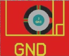
Plum Blossom Pad
1. The fixing hole should be non-metallized. During wave soldering, if the fixing hole is metallized, solder can block the hole during the reflow soldering process.
2. Fixing mounting holes arranged in a quincunx pattern are commonly used for GND networks, as PCB copper is typically used to lay out the GND network. After installing PCB shell components on quincunx holes, GND is effectively connected to the ground. Occasionally, the PCB shell also functions as shielding. However, some designs may not require connecting the mounting hole to the GND network.
3. Metal screw holes may become distorted, leading to grounding issues and unusual system anomalies. Plum blossom holes, regardless of stress variations, can consistently maintain a grounded connection for the screw.
Cross Pattern Pads
Cross pattern pads, also known as thermal pads or hot air pads, help manage heat dissipation during soldering, reducing the risk of soldering defects or PCB damage due to excessive heat.
1. When used for ground pads, cross patterns can reduce the ground wire area, slow down heat dissipation, and facilitate soldering.
2. For PCBs requiring machine placement and reflow soldering, cross pattern pads can help prevent PCB peeling by requiring more heat to melt the solder paste.
Teardrop Pad
A teardrop is an extended connection between a pad and a wire or a wire and a via, designed to protect against external forces that could disconnect the pad or wire. Teardrops also enhance the PCB’s appearance.
1. During soldering, teardrops protect the pad and prevent it from falling off due to repeated soldering.
2. They improve connection reliability by mitigating issues such as uneven etching and cracks caused by via misalignment.
3. Teardrops help smooth impedance transitions and reduce sharp impedance jumps.
In PCB design, to strengthen the pad and prevent disconnections during mechanical processing, a copper film is often used to create a transition area between the pad and the wire. This transition, resembling a teardrop, is commonly referred to as a fill teardrop.

