Copper Coating in PCB Design: Enhancing Performance and Functionality
Introduction
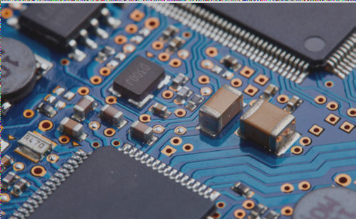
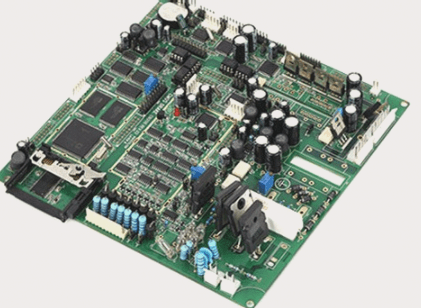
Copper coating, also known as copper pour, is a vital aspect of Printed Circuit Board (PCB) design. It involves filling unused areas of the PCB with solid copper to improve grounding, power distribution, thermal management, and soldering processes. In this article, we explore the key benefits of copper coating and best practices for its application.
What is Copper Pour?
Copper pour is the process of filling unused PCB areas with solid copper, creating a continuous copper area that connects with the ground plane. This technique, also called “copper filling,” offers various electrical and mechanical advantages.
Key Benefits of Copper Coating
-
Improved Grounding and Noise Reduction
Copper coating enhances the PCB’s grounding system, reducing impedance, improving signal integrity, and minimizing electromagnetic interference, crucial for high-frequency circuits.
-
Enhanced Power Distribution
Copper filling ensures efficient power delivery, stabilizing supply voltage and enhancing overall circuit performance.
-
Reduced Loop Area
A well-designed copper pour minimizes unwanted inductive effects and noise coupling by reducing the loop area between power and ground planes.
-
Thermal Management
Copper coating aids in heat dissipation, preventing overheating in high-power applications.
-
Improved Soldering Process
Copper filling helps maintain board stability during soldering, ensuring even heat distribution and reducing the risk of warping.
Potential Pitfalls
While copper coating offers significant advantages, improper application can lead to potential issues:
- Ground Bounce and Noise Issues: Improper copper pours can create unintended loops, causing noise problems.
- Design Complexity and Routing Challenges: Copper pour may complicate PCB design and routing, requiring careful planning to avoid short circuits.
- Manufacturing Challenges: Excessive copper areas can lead to manufacturing difficulties and impact PCB layer alignment.
Best Practices for Copper Pour Application
- Define Clear Zones: Designate areas for copper pour, ensuring proper connections to ground or power planes.
- Ensure Proper Clearance: Maintain adequate space between copper fills and other components to prevent shorts.
- Use a Solid Ground Plane: Opt for a solid ground plane for effective copper pours, avoiding grid-like ground traces.
- Test Design and Simulate: Verify the design and simulate performance to ensure optimal copper coating application.
Benefits of Copper Coating in PCB Design
- Reduces noise
- Improves power distribution
- Enhances thermal management
Before finalizing a PCB design, it’s essential to use simulation tools to verify the effectiveness of the copper pour. This step ensures that the copper coating achieves the desired results without introducing new issues. Signal integrity, power distribution, and thermal performance should be simulated to guarantee optimal functionality.
Challenges in High-Frequency Circuit Design
High-frequency circuits present specific challenges related to noise and interference management on PCBs. The distributed capacitance of PCB traces, especially concerning trace length and frequency, can lead to unwanted noise radiation. Improperly grounded copper pour can exacerbate this issue by acting as a medium for noise propagation.
Optimizing Grounding for High-Frequency Circuits
In high-frequency circuit design, connecting the ground wire to the ground plane is not sufficient. Ground lines should be kept shorter than λ/20, with strategic via placement to ensure a solid connection to the board’s ground plane. Proper grounding and copper pour management can reduce noise and act as a shield against electromagnetic interference.
Copper Pour Techniques: Large Area vs. Grid Copper
There are two primary copper pour techniques: large-area copper and grid copper. Large-area copper is suitable for current handling and shielding, while grid copper is ideal for EMI protection and heat dissipation. Designers must consider the trade-offs between the two techniques based on the circuit’s requirements and operating frequencies.
Best Practices for Copper Pour Implementation
- Ground Segmentation: Isolate multiple ground types and apply copper pour individually for digital and analog grounds.
- Single-Point Grounding: Use 0-ohm resistors or inductors to ensure low-impedance paths between different grounds.
- Crystal Oscillator Considerations: Pour copper around the oscillator to prevent EMI radiation and maintain signal integrity.
- Island (Dead Zone) Issues: Connect isolated copper sections with ground vias to avoid dead zones in large copper pours.
PCB Design Best Practices for Optimal Performance
- Proper Ground Routing: Ground traces should be carefully routed from the start to avoid increased impedance and poor performance.
- Avoid Sharp Corners: Use rounded or curved edges in PCB traces to minimize unwanted electromagnetic signals.
- Avoid Copper Pour in Middle Layer Open Areas: In multilayer boards, refrain from pouring copper in open middle layer areas to ensure proper grounding connection.
- Metal Component Grounding: Ensure metal components like heat sinks are well-grounded to prevent EMI and aid in heat dissipation.
- Thermal Management: Properly ground thermal metal blocks for components like three-terminal regulators to enhance stability and reduce noise.
Latest Developments
Recent studies have shown that incorporating advanced heat dissipation materials in PCB design can significantly improve thermal management and overall performance. By utilizing innovative thermal metal blocks and enhanced isolation strips, designers can effectively reduce noise and ensure stable operation, especially in high-frequency applications.
Conclusion
Effective copper pour techniques and grounding strategies are essential in high-frequency PCB design to minimize electromagnetic interference and enhance circuit performance. Designers must carefully consider factors such as frequency, current, and thermal management when implementing copper pours. By prioritizing proper ground connections, trace routing, and copper pour layout, noise and interference can be significantly reduced, leading to a more reliable and functional PCB.