Methods to Control Signal Crosstalk in High-Speed PCB Design
- With the complexity of system design increasing, designers are now focusing on circuits operating above 100 MHz.
- Approximately 50% of designs operate at frequencies exceeding 50 MHz, with nearly 20% operating at frequencies over 120 MHz.
- Transmission line effects and signal integrity issues arise at 50 MHz, becoming more critical by 120 MHz.
- Sophisticated semiconductor technology accelerates signal transition edges, leading to severe signal integrity and electromagnetic compatibility issues.
- EDA technology enhances circuit design efficiency through automated logic compilation, synthesis, optimization, layout, and simulation.
- Crosstalk, a critical concern, results from mutual inductance and capacitance between signal lines, inducing noise on the line.
- Minimizing signal crosstalk involves strategies such as reducing signal edge transition rates, implementing shielding measures, optimizing layer and wiring configurations, employing distinct wiring layers, and ensuring impedance matching.
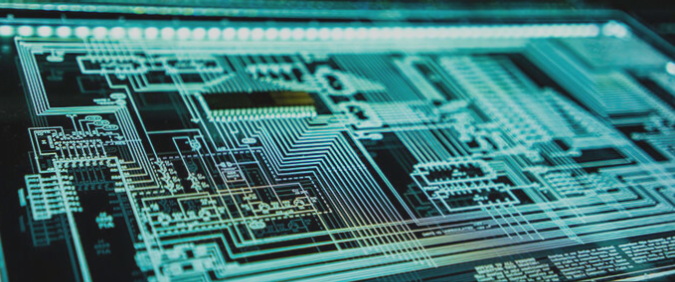
Contemporary electronic product design requires innovative approaches to address signal integrity issues in high-speed digital circuit systems. EDA technology plays a crucial role in enhancing circuit design efficiency and mitigating designer workload. Crosstalk, a critical concern in PCB design, can be minimized through various strategies to ensure optimal signal quality and performance.
Importance of Crosstalk Analysis and Mitigation in PCB Design
Effective crosstalk analysis and mitigation play a crucial role in successful PCB implementation. By integrating simulation tools with PCB layout environments, designers can ensure accurate analysis, apply rules effectively, and continuously refine designs to meet stringent electrical performance standards.
Utilizing Tools for Enhanced Performance
Tools like ICX are invaluable for supporting electrical rule-driven routing. They streamline simulation processes, facilitate in-depth analysis, and automatically adjust designs to uphold precise electrical performance criteria. This integration enhances the overall efficiency and accuracy of the design process.
Key Principles in High-Speed PCB Design
High-speed PCB design principles encompass both physical and electrical rules. While physical rules dictate parameters such as line widths, spacings, and trace lengths, electrical rules are essential for ensuring signal integrity. By controlling factors like wiring delay, crosstalk levels, and signal swings, designers can surpass basic physical specifications and meet stringent performance requirements.
Ensuring Signal Integrity for Optimal Performance
Adhering to both physical and electrical rules is critical in high-speed PCB design. By focusing on signal integrity and preemptively identifying and resolving issues during the design phase, designers can effectively overcome challenges and optimize the performance of modern high-speed system PCB designs.