Preface: PCB Board Reflow Soldering Analysis and Burst Plate Improvement
With the advancement of electronic products toward greater functionality, higher density, miniaturization, and three-dimensional designs, the importance of heat dissipation has increased significantly. Concurrently, thermal stress and warping, resulting from the different Coefficients of Thermal Expansion (CTE) of various materials, have elevated the risk of assembly failures and increased the likelihood of early electronic product failures. Consequently, PCB soldering reliability has become critically important. This document introduces the phenomenon of plate failure during reflow soldering and suggests improvement methods for reference.
1. Plate Burst Phenomenon in Reflow Soldering
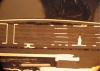
1.1 Definition of Burst Plate: In reflow soldering processes (especially with lead-free applications), a burst plate is defined as the separation phenomenon occurring between the PP layer and the secondary layer (L2) copper foil on the brown surface of HDI multilayer PCBs during the second compression. Analysis of the slices reveals that burst plates often occur in densely buried areas between the first and second layers. No debris or other abnormalities were detected; however, the slices indicate that the burst plate phenomenon is severe, with some second-layer circuits being pulled apart.

1.2 Factors Affecting Board Burst
⑴ Volatile Matter Formation as a Necessary Condition for Explosions
1. **Moisture Absorption Issues**: Water in PCB boards, including diffusion and vapor pressure changes with temperature, reveals that water vapor is the primary cause of PCB explosions. Moisture in PCBs primarily resides in resin molecules and physical defects like voids or micro-cracks. The water absorption rate and equilibrium are influenced by free volume and the concentration of polar groups in epoxy resin. Greater free volume accelerates initial water absorption, while polar groups, which have an affinity for water, contribute to higher equilibrium absorption. Elevated temperatures during lead-free reflow soldering cause water to diffuse outward and accumulate in voids, increasing the molar volume fraction of water. Additionally, as welding temperatures rise, so does the saturated vapor pressure of water, potentially leading to bursts if the bonding strength between material layers is exceeded. Thus, pre-soldering moisture absorption is a key factor in PCB delamination and board burst.
2. **Impact of Moisture During Storage and Production**: HDI multilayer PCBs are moisture-sensitive, with significant performance effects from water presence. For example: (a) Moisture in storage environments alters PP (prepreg) characteristics significantly; (b) PP readily absorbs moisture without protection. Figure 1.3 demonstrates PP’s moisture absorption at different humidity levels and its correlation with storage time. Vacuum packaging results in higher water absorption rates compared to non-vacuum methods. (c) Moisture mainly penetrates resin system interfaces, impacting their properties.
3. **Harm of Moisture Absorption**: (a) Increases volatile content in PP. (b) Moisture weakens cross-linking in PP resin, reducing layer bonding strength and thermal shock resistance, leading to issues like white spots, bubbling, and layer separation during hot oil or solder baths and hot air leveling.
⑵ Poor Adhesion Between PP and Copper Foil as a Sufficient Condition for Board Burst
1. **Phenomenon Description**: Analysis shows that board bursts often occur between the secondary pressing PP and the copper foil’s contact surface. Copper’s non-polar nature means many adhesives have low adhesion to it. Without proper surface treatment, even high-performance adhesives fail to bond adequately. Early browning methods, such as forming Cu2O on the copper foil, increased room-temperature adhesion but led to peeling near 200°C due to Cu2O instability. Toshiba’s 1960s discovery of CuO treatment, creating a stable black velvet-like film, improved adhesion. By the mid-1990s, Europe and the U.S. adopted new chemical oxidation processes for inner conductive patterns, replacing traditional methods and becoming widely used.
2. **Browning Process Enhancements**: The new browning process involves: 2Cu + H2SO4 + H2O2 + nR1 + nR2 → CuSO4 + 2H2O + Cu(R1 + R2). H2O2’s micro-etching effect creates uneven microstructures on copper surfaces, increasing bonding area 6-7 times compared to untreated copper. An organic metal film also forms a strong bond, as SEM images of browned copper show. Adhesive entering the textured areas enhances mechanical engagement.
3. **Factors Affecting Browning Effectiveness**: The quality of browning depends on process parameter control: (a) Advanced formula potions like Atotech provide high roughness, with binding forces withstanding up to 12 times lead-free reflow temperatures. (b) Monitor bath liquid composition during production. (c) Browning (or black copper oxide) film thickness impacts bonding strength, acid/alkali resistance, corona resistance, and temperature tolerance. Thicker films don’t necessarily mean stronger bonds. (d) Contaminated browning layers can cause poor bonding and PCB blistering during SMT assembly. Misuse of high Tg materials in pressing common materials contributes to poor bonding.
⑶ Inappropriate Reflow Temperature Selection as a Predisposing Factor for Board Burst
1. **Temperature Effects**: Analysis shows that plate bursts are temperature-dependent. Increasing reflow soldering temperature raises volatile matter and expansion pressure while decreasing adhesion between browning layers and PP. Therefore, optimizing reflow soldering temperatures based on product characteristics can suppress board bursts.
2. **Optimizing Reflow Soldering Temperature**: (a) Woychik of US Microelectronics Packaging notes that while SnPb alloy tolerates up to 240°C, SnAgCu (lead-free) alloy requires a JEDEC-stipulated 260°C. Higher temperatures may compromise electronic packaging integrity and cause delamination, particularly in moisture-containing laminated materials. (b) JSHwang of American Electronic Assembly Welding suggests a peak temperature of 235°C for lead-free soldering, not exceeding 245°C, to prevent board bursts effectively.
⑷ Poor Escape of Volatile Matter as a Contributing Factor
Analysis shows board bursts commonly occur under large copper foil areas over buried holes. This design flaw exacerbates volatile matter retention and surface temperature unevenness during reflow welding, increasing thermal stress and separation between HDI multilayer PCB layers. Unreasonable design contributes significantly to board bursts in lead-free manufacturing.
1.3 Mechanism of Board Burst
⑴ **Explosion Mechanism**: Based on the analysis, the physical process of board bursts involves: 1. Good bonding between multilayer boards L1-L2 at lower temperatures. 2. As heating progresses, volatile matter like moisture is discharged. 3. Accumulated gases between buried holes and PP (bonding sheet). 4. Increased temperature causes greater gas accumulation near the buried hole, creating expansion pressure that separates L2 and PP. 5. When expansion pressure exceeds the bonding force between the browning surface and PP (F), separation occurs along L2, causing noticeable bubbling and stratification. Improved escape of water vapor through microporous PCB substrates can reduce accumulation in voids or microcracks. However, large copper foil coverage can block vapor escape, increasing board burst likelihood.
1.4 Countermeasures to Prevent Board Explosion
⑴ **Eradicating Plate Explosion**: Prevent PP from absorbing moisture by storing under optimal conditions: temperature (10-20°C), humidity <50%RH, or vacuum. Avoid refrigeration, as it may impact multilayer board quality. Control warehouse conditions, use vacuum and aluminum packaging, and seek new materials with better heat resistance and low moisture absorption.
⑵ **Suppressing Board Explosion**: Optimize the “browning” process and improve adhesion between PCB internal layers. Use high-quality browning potions and monitor raw material quality, including resin content, gel time, fluidity, and volatile content. Ensure resin uniformity and occupancy for low water absorption, better dielectric properties, interlayer adhesion, and dimensional stability.
⑶ **Improving Copper Foil Surface Air Permeability**: Design PCB surfaces with large copper foil areas to allow better water vapor release. This adjustment can help prevent board explosions.
⑷ **Optimizing Reflow Welding Temperature**: Reduce peak reflow temperatures as much as possible while ensuring good wetting to prevent board bursts.
With the advancement of electronic products toward greater functionality, higher density, miniaturization, and three-dimensional designs, the importance of heat dissipation has increased significantly. Concurrently, thermal stress and warping, resulting from the different Coefficients of Thermal Expansion (CTE) of various materials, have elevated the risk of assembly failures and increased the likelihood of early electronic product failures. Consequently, PCB soldering reliability has become critically important. This document introduces the phenomenon of plate failure during reflow soldering and suggests improvement methods for reference.
1. Plate Burst Phenomenon in Reflow Soldering
1.1 Definition of Burst Plate: In reflow soldering processes (especially with lead-free applications), a burst plate is defined as the separation phenomenon occurring between the PP layer and the secondary layer (L2) copper foil on the brown surface of HDI multilayer PCBs during the second compression. Analysis of the slices reveals that burst plates often occur in densely buried areas between the first and second layers. No debris or other abnormalities were detected; however, the slices indicate that the burst plate phenomenon is severe, with some second-layer circuits being pulled apart.

1.2 Factors Affecting Board Burst
⑴ Volatile Matter Formation as a Necessary Condition for Explosions
1. **Moisture Absorption Issues**: Water in PCB boards, including diffusion and vapor pressure changes with temperature, reveals that water vapor is the primary cause of PCB explosions. Moisture in PCBs primarily resides in resin molecules and physical defects like voids or micro-cracks. The water absorption rate and equilibrium are influenced by free volume and the concentration of polar groups in epoxy resin. Greater free volume accelerates initial water absorption, while polar groups, which have an affinity for water, contribute to higher equilibrium absorption. Elevated temperatures during lead-free reflow soldering cause water to diffuse outward and accumulate in voids, increasing the molar volume fraction of water. Additionally, as welding temperatures rise, so does the saturated vapor pressure of water, potentially leading to bursts if the bonding strength between material layers is exceeded. Thus, pre-soldering moisture absorption is a key factor in PCB delamination and board burst.
2. **Impact of Moisture During Storage and Production**: HDI multilayer PCBs are moisture-sensitive, with significant performance effects from water presence. For example: (a) Moisture in storage environments alters PP (prepreg) characteristics significantly; (b) PP readily absorbs moisture without protection. Figure 1.3 demonstrates PP’s moisture absorption at different humidity levels and its correlation with storage time. Vacuum packaging results in higher water absorption rates compared to non-vacuum methods. (c) Moisture mainly penetrates resin system interfaces, impacting their properties.
3. **Harm of Moisture Absorption**: (a) Increases volatile content in PP. (b) Moisture weakens cross-linking in PP resin, reducing layer bonding strength and thermal shock resistance, leading to issues like white spots, bubbling, and layer separation during hot oil or solder baths and hot air leveling.
⑵ Poor Adhesion Between PP and Copper Foil as a Sufficient Condition for Board Burst
1. **Phenomenon Description**: Analysis shows that board bursts often occur between the secondary pressing PP and the copper foil’s contact surface. Copper’s non-polar nature means many adhesives have low adhesion to it. Without proper surface treatment, even high-performance adhesives fail to bond adequately. Early browning methods, such as forming Cu2O on the copper foil, increased room-temperature adhesion but led to peeling near 200°C due to Cu2O instability. Toshiba’s 1960s discovery of CuO treatment, creating a stable black velvet-like film, improved adhesion. By the mid-1990s, Europe and the U.S. adopted new chemical oxidation processes for inner conductive patterns, replacing traditional methods and becoming widely used.
2. **Browning Process Enhancements**: The new browning process involves: 2Cu + H2SO4 + H2O2 + nR1 + nR2 → CuSO4 + 2H2O + Cu(R1 + R2). H2O2’s micro-etching effect creates uneven microstructures on copper surfaces, increasing bonding area 6-7 times compared to untreated copper. An organic metal film also forms a strong bond, as SEM images of browned copper show. Adhesive entering the textured areas enhances mechanical engagement.
3. **Factors Affecting Browning Effectiveness**: The quality of browning depends on process parameter control: (a) Advanced formula potions like Atotech provide high roughness, with binding forces withstanding up to 12 times lead-free reflow temperatures. (b) Monitor bath liquid composition during production. (c) Browning (or black copper oxide) film thickness impacts bonding strength, acid/alkali resistance, corona resistance, and temperature tolerance. Thicker films don’t necessarily mean stronger bonds. (d) Contaminated browning layers can cause poor bonding and PCB blistering during SMT assembly. Misuse of high Tg materials in pressing common materials contributes to poor bonding.
⑶ Inappropriate Reflow Temperature Selection as a Predisposing Factor for Board Burst
1. **Temperature Effects**: Analysis shows that plate bursts are temperature-dependent. Increasing reflow soldering temperature raises volatile matter and expansion pressure while decreasing adhesion between browning layers and PP. Therefore, optimizing reflow soldering temperatures based on product characteristics can suppress board bursts.
2. **Optimizing Reflow Soldering Temperature**: (a) Woychik of US Microelectronics Packaging notes that while SnPb alloy tolerates up to 240°C, SnAgCu (lead-free) alloy requires a JEDEC-stipulated 260°C. Higher temperatures may compromise electronic packaging integrity and cause delamination, particularly in moisture-containing laminated materials. (b) JSHwang of American Electronic Assembly Welding suggests a peak temperature of 235°C for lead-free soldering, not exceeding 245°C, to prevent board bursts effectively.
⑷ Poor Escape of Volatile Matter as a Contributing Factor
Analysis shows board bursts commonly occur under large copper foil areas over buried holes. This design flaw exacerbates volatile matter retention and surface temperature unevenness during reflow welding, increasing thermal stress and separation between HDI multilayer PCB layers. Unreasonable design contributes significantly to board bursts in lead-free manufacturing.
1.3 Mechanism of Board Burst
⑴ **Explosion Mechanism**: Based on the analysis, the physical process of board bursts involves: 1. Good bonding between multilayer boards L1-L2 at lower temperatures. 2. As heating progresses, volatile matter like moisture is discharged. 3. Accumulated gases between buried holes and PP (bonding sheet). 4. Increased temperature causes greater gas accumulation near the buried hole, creating expansion pressure that separates L2 and PP. 5. When expansion pressure exceeds the bonding force between the browning surface and PP (F), separation occurs along L2, causing noticeable bubbling and stratification. Improved escape of water vapor through microporous PCB substrates can reduce accumulation in voids or microcracks. However, large copper foil coverage can block vapor escape, increasing board burst likelihood.
1.4 Countermeasures to Prevent Board Explosion
⑴ **Eradicating Plate Explosion**: Prevent PP from absorbing moisture by storing under optimal conditions: temperature (10-20°C), humidity <50%RH, or vacuum. Avoid refrigeration, as it may impact multilayer board quality. Control warehouse conditions, use vacuum and aluminum packaging, and seek new materials with better heat resistance and low moisture absorption.
⑵ **Suppressing Board Explosion**: Optimize the “browning” process and improve adhesion between PCB internal layers. Use high-quality browning potions and monitor raw material quality, including resin content, gel time, fluidity, and volatile content. Ensure resin uniformity and occupancy for low water absorption, better dielectric properties, interlayer adhesion, and dimensional stability.
⑶ **Improving Copper Foil Surface Air Permeability**: Design PCB surfaces with large copper foil areas to allow better water vapor release. This adjustment can help prevent board explosions.
⑷ **Optimizing Reflow Welding Temperature**: Reduce peak reflow temperatures as much as possible while ensuring good wetting to prevent board bursts.


