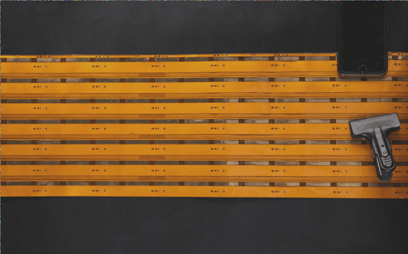
High-density FPC represents a segment of the broader FPC category, typically defined as having a line pitch of less than 200μm or a microvia diameter of less than 250μm. This type of FPC finds extensive applications across various sectors, including telecommunications, computing, integrated circuits, and medical devices.
The distinctive features of FPC enable it to serve as an alternative to rigid circuit boards and traditional wiring methods in many scenarios, fostering innovation in several emerging fields. One of the fastest-growing applications for FPC is in the internal connection lines of computer hard disk drives (HDDs). The magnetic head in a hard disk must traverse the rotating disk to perform scanning functions, and flexible circuits can replace conventional wires to connect the moving magnetic head with the control circuit board. Hard disk manufacturers employ a technology known as “floating flexible board” (FOS) to enhance production efficiency and reduce assembly costs. Moreover, wireless suspension technology provides improved shock resistance, thereby increasing product reliability. Another type of high-density FPC utilized in hard drives is the interposer flex, which is positioned between the suspension and the controller.

1. FPC’s growth rate ranks second in the new integrated circuit packaging sector. Chip-scale packaging (CSP), multi-chip modules (MCM), and chip-on-FPC (COF) all utilize flexible circuits. Notably, the market for CSP interconnect circuits is particularly significant, as they are employed in semiconductor devices and flash memory. These technologies are widely found in PCMCIA cards, disk drives, personal digital assistants (PDAs), mobile phones, pagers, digital video cameras, and digital cameras. Additionally, liquid crystal displays (LCDs), polyester membrane switches, and inkjet printer cartridges represent three other high-growth application areas for high-density FPCs.
2. The market potential for flexible circuit technology in portable devices, such as mobile phones, is substantial. This demand arises from the necessity for small size and light weight to satisfy consumer preferences. Furthermore, the latest applications of flexible technology include flat panel displays and medical equipment, allowing designers to reduce the size and weight of products like hearing aids and implantable devices.
3. Lasers play three primary roles in the FPC manufacturing process: forming (cutting and shaping), slicing, and drilling. As a non-contact processing tool, lasers can apply high-intensity light energy (650 mW/mm²) to a small focal area (100–500 μm). This intense energy is effective for cutting, drilling, and working with materials. Processing speed and quality depend on the properties of the material being processed and the characteristics of the laser, such as wavelength, energy density, peak power, pulse width, and frequency. FPC processing commonly utilizes ultraviolet (UV) and far-infrared (FIR) lasers, with excimer or UV diode-pumped solid-state (UV-DPSS) lasers typically employed for the former, while sealed CO2 lasers are used for the latter.
4. **Processing and Molding**
Laser processing is known for its high precision and broad applicability, making it an ideal tool for FPC molding. Whether using a CO2 or DPSS laser, materials can be shaped into various forms after focusing. A mirror is installed on a galvanometer to direct the focused laser beam anywhere on the workpiece’s surface (Figure 1). Vector scanning technology allows for computer numerical control (CNC) of the galvanometer, with CAD/CAM software used to generate cutting graphics. This “soft tool” facilitates real-time laser control when design changes are made. By adjusting the light zoom and cutting tools, laser processing can accurately reproduce design graphics, which is a significant advantage.
5. **Drilling**
Although some facilities still employ mechanical drilling, stamping, or plasma etching for micro-via formation, laser drilling remains the most widely used method for creating micro-vias in FPCs due to its high productivity, flexibility, and extended uptime.
6. Mechanical drilling and punching utilize high-precision drills and dies to create holes approximately 250 μm in diameter in FPCs. However, this high-precision equipment is costly and has a limited lifespan. Since the hole diameters required for high-density FPCs are often less than 250 μm, mechanical drilling is not preferred.
7. Plasma etching can produce micro-vias smaller than 100 μm on a 50 μm thick polyimide film substrate, but the equipment and process costs are significant. Maintenance costs for plasma etching are also high, especially concerning chemical waste processing and consumables. Additionally, establishing a new process for consistent and reliable micro-via production can be time-consuming. Despite these drawbacks, plasma etching is known for its high reliability, with reports indicating a qualified rate of 98%. As a result, it maintains a niche market in medical and avionics applications.
8. In contrast, laser-based micro-via creation is straightforward and cost-effective. The initial investment in laser equipment is low, and as a non-contact tool, it eliminates the costly tool replacement associated with mechanical drilling. Moreover, modern sealed CO2 and UV-DPSS lasers require minimal maintenance, reducing downtime and significantly enhancing productivity.
9. The process for producing micro-vias in FPCs is similar to that for rigid PCBs. However, variations in substrate and thickness necessitate adjustments to critical laser parameters. Both sealed CO2 and UV-DPSS lasers can employ the same vector scanning technology as in the molding process for direct drilling on FPCs. The only difference lies in the drilling application software, which scans the mirror from one micro-via to the next. The laser is turned off during movement and activated only when reaching the next drilling position. To ensure holes are perpendicular to the FPC substrate’s surface, the laser beam must be directed vertically, achievable through a telecentric lens system positioned between the scanning mirror and the substrate.
10. CO2 lasers can also utilize conformal mask technology for micro-via drilling. In this method, the copper surface serves as a mask, with holes initially etched using conventional printing and etching techniques. Then, a CO2 laser beam is applied to the holes in the copper foil to remove the exposed dielectric materials.
11. Another technique for creating micro-vias involves using an excimer laser with a projection mask. This technology requires mapping an image of a micro-via or an entire micro-via array onto the substrate, after which the excimer laser beam is directed at the mask to transfer the pattern onto the substrate’s surface. Although excimer laser drilling offers excellent quality, its disadvantages include slower speeds and higher costs.
12. **Laser Selection**
While the laser types used for processing FPCs are similar to those for rigid PCBs, differences in material and thickness significantly impact processing parameters and speeds. Occasionally, excimer lasers and lateral excitation gas (TEA) CO2 lasers can be used, but their slower speeds and high maintenance costs can hinder productivity increases. In contrast, CO2 and UV-DPSS lasers are favored for producing and processing FPC micro-vias due to their speed, cost-effectiveness, and wide application.
13. **CO2 Laser (Automation Alternatives)**
Sealed CO2 lasers emit FIR lasers at wavelengths of 10.6 μm or 9.4 μm. Both wavelengths are readily absorbed by dielectrics like polyimide film substrates; however, research indicates that processing with a wavelength of 9.4 μm yields significantly better results. This wavelength exhibits a higher absorption coefficient, facilitating faster drilling or cutting than the 10.6 μm wavelength. The 9.4 μm laser not only excels in drilling and cutting but also demonstrates exceptional slicing capabilities. Therefore, utilizing shorter wavelength lasers enhances FPC productivity and quality.
14. **UV-DPSS Laser**
Both dielectric materials and copper easily absorb UV-DPSS lasers with an output wavelength of 355 nm. UV-DPSS lasers produce smaller spots and have lower output power compared to CO2 lasers. For processing dielectrics, UV-DPSS lasers are typically employed for smaller features (less than 50 μm) on high-density FPC substrates. For micro-vias, UV lasers are ideal. High-power UV-DPSS lasers are now available, capable of increasing both processing and drilling speeds.
15. Materials with higher UV etching thresholds, like copper, require high-energy, low-repetition-rate lasers, while low-threshold materials, such as polyimide films, necessitate low-energy, high-repetition-rate lasers. This approach minimizes damage to copper pads and enhances productivity. To optimize production capacity, most larger diameter micro-vias are processed in two stages: initially using a UV-DPSS laser to drill through the copper foil, followed by a CO2 laser to remove the exposed dielectric.


