The Importance of PCB Layout in Engineering
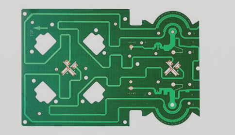
When it comes to PCB layout, experience plays a crucial role in navigating the complexities of design. Seasoned PCB engineers, with their extensive exposure to various challenges, can anticipate potential issues and make informed decisions. While some may feel uncertain about certain layouts, skilled engineers combine logic and creativity to tackle design obstacles.
Understanding PCB Basics
PCBs are classified based on layers, with single-layer, double-layer, and multi-layer boards being common types. Single-layer boards are outdated, while double-layer boards are used in audio systems and basic designs like mobile power amplifiers. Multi-layer boards, with four or more layers, offer lower component density. Vias, such as through-hole, blind, and buried vias, play a crucial role in connecting layers.

Efficient Routing Techniques
Prior to manual routing, interactive routing helps manage high-frequency lines, preventing signal reflections. Ground wires can be added to reduce interference, and perpendicular routing of adjacent layers minimizes parasitic coupling. Meticulous planning, setting routing rules, and optimizing paths are essential for successful manual routing.
Signal Isolation and Component Organization
Isolating signals and components is key to a well-organized layout. Low-speed traces should be kept away from high-speed traces, and digital ground should be separate from analog ground to prevent interference. Proper wiring between power and ground, along with wide power and ground traces, enhances system stability and efficiency.
Decoupling capacitors play a crucial role in supplying high current to chips and filtering out power supply noise. Ground planes, wide traces, and efficient integration of power, ground, digital, and analog circuits are essential for multilayer boards.
Proper Grounding Techniques in PCB Design
When designing PCBs, it is essential to consider the interaction between digital and analog circuits. Signal lines should be routed away from sensitive analog components to prevent interference. The ground plane, typically on the surface, plays a crucial role in maintaining a single ground node.
Special attention is required to manage the common ground connection between digital and analog circuits. While these grounds are isolated within the board, they are connected at a single point where the PCB interfaces with external components like connectors. This connection must be carefully handled to prevent interference and ensure proper functioning of the circuits.
Proper isolation and grounding techniques are vital for the overall layout of the system and to avoid signal integrity issues.
- High frequency digital circuits
- Sensitivity of analog circuits
- Ground plane placement
- Single ground node
- Common ground connection
If you require PCB manufacturing services or have any questions about PCB design, feel free to contact us.


