Optimizing Shape Processing Methods for Ultra-Small Circuit Boards
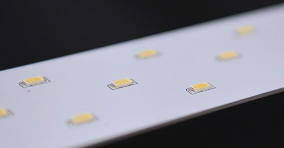
As circuit board technology advances, there is still a demand for simpler circuits, especially ultra-small boards with dimensions as small as 3-4mm. Designing positioning holes for these tiny boards can be challenging, leading to issues like edge bumps and dust accumulation. To address these challenges, a detailed study and experimentation on producing ultra-small circuit boards have been conducted to improve shape processing methods and enhance production efficiency.
Impact of Shape Processing Methods
The choice of shape processing methods plays a crucial role in controlling shape tolerance, reducing processing costs, and improving efficiency. The two most common methods currently used are milling and die cutting.
1. Milling Profile
Milling is known for providing good appearance quality and high dimensional accuracy. However, due to the small dimensions of ultra-small boards, achieving precise control over the milling profile can be difficult. Constraints related to cutter sizes and cutting speeds can limit production efficiency and increase costs. This method is best suited for low-volume production with simple designs.
1.1 Milling Profile Challenges
- Small cutter dimensions
- Restricted cutting speeds
- Low production efficiency
1.2 Die Cutting
For large volumes of small-size PCBs, die cutting can be more efficient than milling despite higher costs. Die cutting is essential for achieving right angles in internal gong grooves and meeting shape tolerance demands.
Experimental Design and Process
Extensive research and experiments have been conducted on milling profile processing methods, die cutting, V-CUT, and more to optimize the production of ultra-small circuit boards.
2. Experimental Design Overview
Based on industry experience, research focused on improving milling profile processing methods and die cutting techniques to enhance production efficiency.
3. Experimental Process Details
Various schemes were tested to optimize shape processing methods:
3.1 Scheme One – Gong Machine Milling Shape
Optimizing gong machining processes to reduce bumps and burrs, ensuring a more precise and efficient production process.
3.2 Scheme Two – Precision Engraving Machine Milling Shape
Utilizing precision engraving machines to minimize bump production and enhance the quality of ultra-small circuit boards.
3.3 Scheme Three – Laser Shape Effect Verification
Testing the effects of laser outlining on ultra-small circuit boards to achieve precise and consistent shapes.
If you have any further questions or need adjustments, feel free to reach out!
Experimental Results
The laser-contoured finished board showed no bumps, meeting size requirements. However, carbon black contamination from laser contouring remained on the board surface, proving difficult to clean with plasma or alcohol wiping methods (refer to Figure 7). This issue resulted in failure to meet customer expectations.
Scheme Four – Die Effect Verification
Die processing ensures the accuracy of size and shape for stamped parts without creating bumps (see Figure 8). Nevertheless, there is a risk of abnormal board corner crushing during processing, which is deemed unacceptable.
Conclusion
This article tackles challenges faced in high-precision small-size circuit boards with a tolerance of +/-0.1 mm. By implementing a rational engineering data design and choosing appropriate processing techniques based on circuit board materials and customer specifications, many challenges can be effectively tackled.