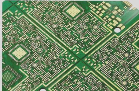
The etching process is a critical step in PCB (Printed Circuit Board) production. In simple terms, the process involves covering the base copper with a resist layer, and then exposing the copper not covered by the resist to an etching solution. The exposed copper reacts with the etchant and is “bitten off,” leaving behind the desired circuit pattern and bonding pads. While this principle is straightforward, implementing etching technology in actual PCB production is quite challenging. This is particularly true for fine-line production, which requires extremely precise line width tolerances and an error-free etching process. Achieving the perfect etching result is crucial; the lines must not be too wide or over-etched.
To better understand the etching process, it’s important to note that many PCB manufacturers prefer using horizontal etching lines for production. This method maximizes automation, thereby reducing production costs. However, horizontal etching is not without its drawbacks. One of the major issues is the “pool effect,” which can lead to uneven etching results on the upper and lower surfaces of the board. The etching rate is faster at the edges of the board than at the center, sometimes causing significant differences in the final etching pattern.
The “pool effect” occurs because the etchant tends to flow out more easily at the edges of the PCB, where it is exposed to more circulation. In contrast, the center of the board experiences slower etching due to restricted etchant flow and reduced exchange between old and new etching solutions. This results in over-etching at the edges and under-etching at the center. Even attempts to compensate for this by slightly widening the circuit on the edges can fail, as the etching tolerances must be very finely controlled to achieve ultra-fine lines.
The root cause of the “pool effect” lies in the circulation dynamics of the etching solution. At the board’s edge, the etching solution is more likely to flow off the board, ensuring that the solution remains fresh and the etching process maintains a consistent rate. However, in the center of the PCB, the etchant becomes more stagnant, and the flow of copper-rich solution is restricted. This leads to reduced etching efficiency and suboptimal etching results. Unfortunately, the “pool effect” is nearly impossible to avoid in practical applications due to the limitations of chain-type horizontal transmission rollers, which inhibit the proper discharge of etching solution, allowing it to accumulate between the rollers.
In conclusion, while horizontal etching offers benefits in terms of automation and cost reduction, the challenges posed by the “pool effect” and the difficulty in achieving precise etching results must be carefully managed. Understanding the underlying mechanics of the etching process and continuously refining the technology is essential for maintaining high-quality, accurate PCBs.

In large-scale PCB production, especially when dealing with ultra-fine lines, achieving consistent etching quality can be a challenge. Even with advanced process controls and compensations, such as adjustable spray systems, oscillating spray pipes, and corrective re-etching sections, these issues persist unless substantial technical investments are made. The goal, however, is to eliminate the “pool effect” without restarting the process from scratch.
At the end of last year, PILL e.K. introduced a new process technology aimed at addressing this problem. By utilizing a vacuum etching method, the fluidity of the etching solution on the board’s surface is improved. This is achieved by using a water pump to suck the used etching solution, which helps prevent the formation of puddles. This method, named vacuum etching, was first demonstrated publicly at Productronica in November 2001. Subsequent tests conducted by PCB manufacturers confirmed that vacuum etching results in excellent, uniform etching with minimal effort required for engineering control.
### Principle and Mechanism of Vacuum Etching
Vacuum etching technology operates on a straightforward principle. Nozzles are installed in the etching section, and air extraction units are positioned between the nozzles, placed close to the surface of the PCB. These extraction units draw away the used etching solution, returning it to the liquid tank through a closed-loop system. The vacuum, or negative pressure, created in the system is carefully calibrated to avoid the formation of the puddle effect, without affecting the production of thin inner layers. By connecting the aspiration system to the fixed upper reel in the conveyor, the distance between the suction and the PCB surface remains optimal, ensuring consistent etching results, regardless of board thickness.
In practice, even on a large 24″ x 24″ board, only a 1-micron copper thickness fluctuation was detected, demonstrating that the etching effect is uniform across both the top and bottom surfaces of the board. Additionally, the overall circuit quality produced by this technology is impressive. Tests with various PCB manufacturers have shown that vacuum etching produces straighter conductor profiles, ensuring that the boards meet precise wiring requirements.
### Factors Affecting Etching Performance
It is important to note that several factors, beyond the vacuum etching process itself, can influence etching quality. These include resist thickness, exposure quality, development process, and the copper thickness of the substrate. While the etching solution renewal cycle or the process parameters account for a significant portion of the etching result, PILL project manager Oliver Briel emphasized that they have successfully controlled this 50% of the process to ensure consistently good results.
### Advantages of Vacuum Etching
1. **Improved Etching Efficiency:** Vacuum etching increases the etching speed, reducing production time and enhancing throughput.
2. **No Need for Rework:** The etching process produces satisfactory results in the first pass, eliminating the need for re-etching or additional rework.
3. **Cost Efficiency:** This technology reduces the need for complex process controls, thereby lowering production costs.
4. **Simplicity in Design:** The use of a vacuum etching system eliminates the need for swingable jet manifolds or nozzles with adjustable spray pressures, which were previously necessary to mitigate the puddle effect.
5. **Compact and Integrated System:** The vacuum etching system combines the suction and etching processes in a single, compact module, making the process more efficient and space-saving.
6. **Optimized Nozzle Arrangement:** Unlike traditional spray manifolds, which are typically arranged longitudinally, vacuum etching nozzles can be arranged laterally along the conveyor’s direction. This setup allows for better maintenance access, reduced downtime for nozzle replacements, and the ability to perform real-time electrical flow monitoring, which helps detect and address issues quickly.
### Potential for Future Development
Vacuum etching holds significant potential, particularly for producing thin or ultra-fine wire structures. Early tests on conductive patterns smaller than 50 microns have shown promising results. Additionally, further evaluations are being conducted on the use of vacuum etching for producing thick copper circuits. The process is also compatible with different etching media. For example, in tests using iron chloride (a common etchant in Asia), results showed improved conductor profiles, especially with steeper angles. This offers a viable alternative to traditional copper chloride-based etching, which could be beneficial for producing fine lines or special features in PCB manufacturing.
In conclusion, vacuum etching technology is poised to revolutionize PCB production, offering enhanced precision, cost efficiency, and flexibility for future advancements in the field.
To better understand the etching process, it’s important to note that many PCB manufacturers prefer using horizontal etching lines for production. This method maximizes automation, thereby reducing production costs. However, horizontal etching is not without its drawbacks. One of the major issues is the “pool effect,” which can lead to uneven etching results on the upper and lower surfaces of the board. The etching rate is faster at the edges of the board than at the center, sometimes causing significant differences in the final etching pattern.
The “pool effect” occurs because the etchant tends to flow out more easily at the edges of the PCB, where it is exposed to more circulation. In contrast, the center of the board experiences slower etching due to restricted etchant flow and reduced exchange between old and new etching solutions. This results in over-etching at the edges and under-etching at the center. Even attempts to compensate for this by slightly widening the circuit on the edges can fail, as the etching tolerances must be very finely controlled to achieve ultra-fine lines.
The root cause of the “pool effect” lies in the circulation dynamics of the etching solution. At the board’s edge, the etching solution is more likely to flow off the board, ensuring that the solution remains fresh and the etching process maintains a consistent rate. However, in the center of the PCB, the etchant becomes more stagnant, and the flow of copper-rich solution is restricted. This leads to reduced etching efficiency and suboptimal etching results. Unfortunately, the “pool effect” is nearly impossible to avoid in practical applications due to the limitations of chain-type horizontal transmission rollers, which inhibit the proper discharge of etching solution, allowing it to accumulate between the rollers.
In conclusion, while horizontal etching offers benefits in terms of automation and cost reduction, the challenges posed by the “pool effect” and the difficulty in achieving precise etching results must be carefully managed. Understanding the underlying mechanics of the etching process and continuously refining the technology is essential for maintaining high-quality, accurate PCBs.
In large-scale PCB production, especially when dealing with ultra-fine lines, achieving consistent etching quality can be a challenge. Even with advanced process controls and compensations, such as adjustable spray systems, oscillating spray pipes, and corrective re-etching sections, these issues persist unless substantial technical investments are made. The goal, however, is to eliminate the “pool effect” without restarting the process from scratch.
At the end of last year, PILL e.K. introduced a new process technology aimed at addressing this problem. By utilizing a vacuum etching method, the fluidity of the etching solution on the board’s surface is improved. This is achieved by using a water pump to suck the used etching solution, which helps prevent the formation of puddles. This method, named vacuum etching, was first demonstrated publicly at Productronica in November 2001. Subsequent tests conducted by PCB manufacturers confirmed that vacuum etching results in excellent, uniform etching with minimal effort required for engineering control.
### Principle and Mechanism of Vacuum Etching
Vacuum etching technology operates on a straightforward principle. Nozzles are installed in the etching section, and air extraction units are positioned between the nozzles, placed close to the surface of the PCB. These extraction units draw away the used etching solution, returning it to the liquid tank through a closed-loop system. The vacuum, or negative pressure, created in the system is carefully calibrated to avoid the formation of the puddle effect, without affecting the production of thin inner layers. By connecting the aspiration system to the fixed upper reel in the conveyor, the distance between the suction and the PCB surface remains optimal, ensuring consistent etching results, regardless of board thickness.
In practice, even on a large 24″ x 24″ board, only a 1-micron copper thickness fluctuation was detected, demonstrating that the etching effect is uniform across both the top and bottom surfaces of the board. Additionally, the overall circuit quality produced by this technology is impressive. Tests with various PCB manufacturers have shown that vacuum etching produces straighter conductor profiles, ensuring that the boards meet precise wiring requirements.
### Factors Affecting Etching Performance
It is important to note that several factors, beyond the vacuum etching process itself, can influence etching quality. These include resist thickness, exposure quality, development process, and the copper thickness of the substrate. While the etching solution renewal cycle or the process parameters account for a significant portion of the etching result, PILL project manager Oliver Briel emphasized that they have successfully controlled this 50% of the process to ensure consistently good results.
### Advantages of Vacuum Etching
1. **Improved Etching Efficiency:** Vacuum etching increases the etching speed, reducing production time and enhancing throughput.
2. **No Need for Rework:** The etching process produces satisfactory results in the first pass, eliminating the need for re-etching or additional rework.
3. **Cost Efficiency:** This technology reduces the need for complex process controls, thereby lowering production costs.
4. **Simplicity in Design:** The use of a vacuum etching system eliminates the need for swingable jet manifolds or nozzles with adjustable spray pressures, which were previously necessary to mitigate the puddle effect.
5. **Compact and Integrated System:** The vacuum etching system combines the suction and etching processes in a single, compact module, making the process more efficient and space-saving.
6. **Optimized Nozzle Arrangement:** Unlike traditional spray manifolds, which are typically arranged longitudinally, vacuum etching nozzles can be arranged laterally along the conveyor’s direction. This setup allows for better maintenance access, reduced downtime for nozzle replacements, and the ability to perform real-time electrical flow monitoring, which helps detect and address issues quickly.
### Potential for Future Development
Vacuum etching holds significant potential, particularly for producing thin or ultra-fine wire structures. Early tests on conductive patterns smaller than 50 microns have shown promising results. Additionally, further evaluations are being conducted on the use of vacuum etching for producing thick copper circuits. The process is also compatible with different etching media. For example, in tests using iron chloride (a common etchant in Asia), results showed improved conductor profiles, especially with steeper angles. This offers a viable alternative to traditional copper chloride-based etching, which could be beneficial for producing fine lines or special features in PCB manufacturing.
In conclusion, vacuum etching technology is poised to revolutionize PCB production, offering enhanced precision, cost efficiency, and flexibility for future advancements in the field.