**Layer configuration**
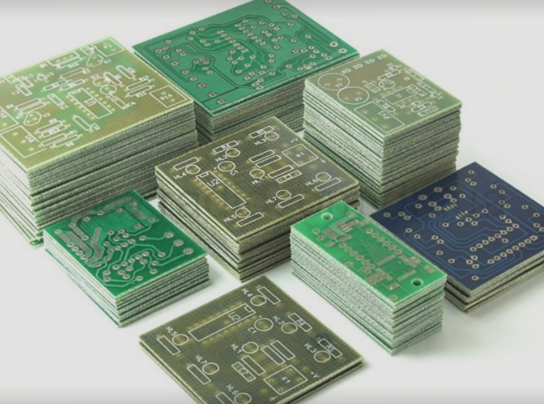
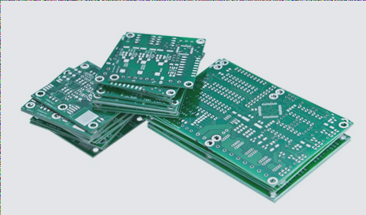
The hierarchy of PCB board mainly includes power layer, ground layer, and signal layer, and the total number of layers is the sum of the quantities of each layer. In the design process, the first step is to organize and classify all power sources, grounding, and various signals, and arrange and design them based on the classification. Normally, different power sources should be divided into different layers, and different grounding planes should also have corresponding grounding planes. Various special signals, such as high-frequency clock signals, require separate design and the addition of a ground plane to shield the special signals, thereby improving electromagnetic compatibility. Of course, cost is also one of the factors that needs to be considered. In the design process, a balance should be found between the electromagnetic compatibility and cost of the system. The primary consideration in the design of a power plane is the type and quantity of power sources. If there is only one power source, a single power layer can be considered. Under high power requirements, multiple power layers can also be used to supply power to devices in different layers. If there are multiple power sources, you can consider designing multiple power layers or dividing different power sources within the same power layer. The premise of division is that there is no crossover between power sources, otherwise multiple power layers must be designed. The design of the number of signal layers should consider the characteristics of all signals. The layering and shielding of special signals are issues that need to be considered. Usually, design is first done using design software, and then modified based on specific details. The layer design must consider both signal density and the integrity of special signals. For special signals, if necessary, a grounding plane layer must be designed as a shield. Generally speaking, single-sided or double-sided designs are not recommended unless purely for cost considerations. Although single-sided and double-sided panel processing is simple and cost-effective, in situations with high signal density and complex signal structures, such as high-speed digital circuits or analog-to-digital hybrid circuits, the circuit area increases and radiation also increases due to the lack of a dedicated reference ground layer on the single panel. Due to the lack of effective shielding, the anti-interference ability of the system will also decrease. After determining the signal and hierarchy, the layout design of each layer of the PCB board also needs to be scientifically designed.
**The middle layer layout design of PCB board follows the following principles:**
1. Place the power plane adjacent to the corresponding ground plane. The purpose of this design is to form a coupling capacitor that works together with the decoupling capacitor on the PCB to reduce the impedance of the power plane and achieve a wider filtering effect.
2. The selection of reference layer is very important. In theory, both the power layer and the ground plane can be used as reference layers, but the ground plane can usually be grounded, so its shielding effect is much better than that of the power layer. Therefore, it is usually recommended to choose the grounding plane as the reference layer.
3. The key signals of two adjacent layers cannot cross the partition. Otherwise, it will form a large signal loop, leading to strong radiation and coupling.
4. To maintain the integrity of the grounding plane, signal lines shall not be arranged on the grounding plane. If the signal line density is too high, it is possible to consider wiring at the edge of the power plane.
5. The grounding layer should be designed below key signals such as high-speed signals, guidance signals, and high-frequency signals to ensure the shortest signal circuit path and minimum radiation.
6. In the process of high-speed circuit design, it is necessary to consider the radiation of the power supply and the interference to the entire system. Usually, the area of the power plane should be smaller than that of the ground plane so that the ground plane can shield the power supply. Generally, it is required that the power plane shrinks inward by twice the thickness of the dielectric. If you want to reduce the contraction of the power plane, you need to minimize the thickness of the medium as much as possible.
**The general principles that should be followed in the layout design of multi-layer printed circuit boards are:**
1. The power plane should be close to the ground plane and designed below the ground plane.
2. The wiring layer should be designed to be adjacent to the entire metal plane.
3. Digital signals and analog signals should be designed for isolation. Firstly, it is necessary to avoid having digital signals and analog signals on the same layer. If unavoidable, digital and analog signals can be wired in different areas and isolated from each other through methods such as slotting. The same applies to analog and digital power supplies. Especially for digital power supplies, their radiation is significant and must be isolated and shielded.
4. The printed circuit in the middle layer forms a planar waveguide, while the surface layer forms a microstrip line. The transmission characteristics of the two are different.
5. Clock circuits and high-frequency circuits are the main sources of interference and radiation, and must be arranged separately and kept away from sensitive circuits.
6. The stray current and high-frequency radiation current contained in different layers are different, and cannot be generalized when wiring.
The electromagnetic compatibility of PCB boards can be greatly improved through layer design and layout. The layer design mainly considers power and ground layers, high-frequency signals, special signals, and sensitive signals. The layer layout mainly considers various coupling, grounding and power line layouts, clock and high-speed signal layouts, analog signal and digital information layouts.


