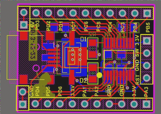
In PCB design, the concept of pads is paramount, and PCB engineers must grasp it thoroughly. However, despite being acquainted with it, many engineers only possess a partial understanding of pads. Below, we will delve into the various types and design standards of pads in PCB design.
Generally, pads can be categorized into seven types, distinguished by their shapes as follows:
1. **Square Pad:** These are suited for printed boards with few, large components and simple printed wires. They facilitate ease of use, particularly when crafting PCBs manually.
2. **Circular Pad:** Widely employed in single and double-sided printed boards featuring a regular component arrangement. If the board’s density allows, larger pads can be utilized to ensure secure soldering.
3. **Island Pad:** Integration characterizes the connection between pads. They find frequent application in vertically irregular alignment installations, such as those in cassette recorders.
4. **Teardrop Pad:** Employed when thin wires are connected to prevent peeling and wire disconnection from the pad, especially prevalent in high-frequency circuits.
5. **Polygonal Pad:** These pads serve to differentiate between pads with closely spaced outer diameters and varying apertures, facilitating processing and assembly.
6. **Oval Pad:** Offering ample area to enhance strip-resistance, they are commonly used in double-line inserts.
7. **Open-End Pad:** Ensures that after wave soldering, manually repaired soldering pad holes remain unclosed by soldering tin.

