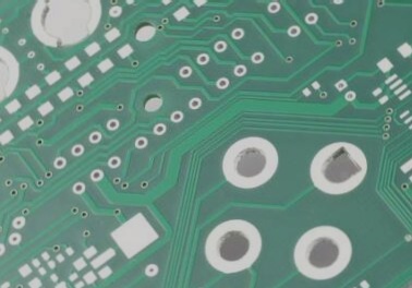
Electrical Testing in PCB Manufacturing
Importance of Electrical Testing
During the production of PCB boards, electrical defects such as short circuits, open circuits, and leakage can occur due to various factors. With the advancement of PCB designs towards high density and complexity, it is crucial to detect and rectify defects early to minimize cost wastage. Enhancing testing technologies alongside process control improvements can lead to reduced scrap rates and improved product yields for PCB manufacturers.
Cost Impact of Defects
In the manufacturing of electronic products, the cost incurred due to defects varies at each stage of production. Detecting defects early is key to minimizing costs. For PCB boards, the “Rule of 10’s” is used to evaluate costs associated with addressing defects at different stages. Timely detection of defects, such as open circuits, can prevent additional costs incurred during downstream assembly processes.
Role of Electrical Testing
Electrical testing plays a crucial role in identifying boards with functional circuit defects promptly. Downstream manufacturers often require PCB board manufacturers to perform 100% electrical testing to ensure quality. Testing is necessary at key stages of PCB manufacturing to identify and rectify defective boards, ultimately improving product quality.
Methods and Equipment for Electrical Measurement
Various electrical testing methods exist, including Dedicated Test, Universal Grid Test, Flying Probe Test, and more. Each method has its unique features and capabilities, catering to different testing requirements. Understanding the characteristics of each testing method and equipment can help in selecting the most suitable approach for PCB testing.
Key Testing Stages
- After etching the inner layer
- After etching the outer layer circuit
- Upon completion of the finished product
Testing Equipment Comparison
- Dedicated Test: Specific to a part number, limited test density
- Universal Grid Test: Allows testing of multiple part numbers, high test point density
- Flying Probe Test: Involves moving probes for testing, suitable for high-density boards
Conclusion
Implementing effective electrical testing methods and equipment in PCB manufacturing is essential for ensuring product quality, reducing costs, and enhancing overall efficiency in the production process.
Technical Comparison
Flying Probe Testing vs. Bed-of-Nails Testing
Flying probe tests typically result in 1-20 yields. The test area’s size varies greatly based on board density and spacing, with high-density boards requiring slower testing speeds. Flying probe testers can cover 3,000 to 5,000 square meters per year.
While Bed-of-Nails test equipment is less common for high-density boards, it can theoretically offer higher output. In practice, special-purpose test equipment is more prevalent in mass production, while general-purpose types are preferred for smaller productions.
Testing costs typically represent only about 2-4% of the total price, making general-purpose and special-purpose models popular choices for mass production. As electronic product designs evolve rapidly, the selection of testing equipment must adapt to shorten product life cycles.

