1. **PCB Factory Process Factors:**
1. **Excessive Etching of Copper Foil**
The electrolytic copper foils used in the market are generally single-sided galvanized (commonly referred to as “ashing foil”) and single-sided copper-plated (known as “red foil”). The standard copper foils are typically galvanized copper foil over 70µm, red foil, and 18µm thickness. Ashing foils usually don’t experience copper rejection in large batches. When the circuit design is optimized for the etching line, any change in copper foil specifications without adjusting the etching parameters can result in the copper foil remaining in the etching solution for too long.
Since zinc is a highly reactive metal, prolonged immersion of the PCB’s copper traces in the etching solution can cause excessive side etching of the traces. This leads to the complete reaction and detachment of the thin zinc layer, causing the copper traces to fall off.
Another scenario involves no issues with the etching parameters themselves, but poor washing and drying after etching. If residual etching solution remains on the PCB surface, it can corrode the copper traces over time. Extended exposure to the residual solution leads to excessive side etching.
This issue typically affects thin traces, and during humid weather, similar defects can appear across the entire PCB. If you peel off the copper trace, you’ll notice that the contact surface with the substrate (the so-called roughened surface) has changed. It will look different from normal copper foil, revealing the original copper color of the base layer. In contrast, copper traces in thicker lines will exhibit normal peeling strength, unaffected by this corrosion.
2. **Mechanical Damage During PCB Production**
In the production process, local collisions can occur that separate the copper trace from the substrate due to mechanical external forces. This type of defect typically results from misalignment during manufacturing. The copper traces may show visible twisting, scratches, or directional impact marks. Upon peeling the copper trace from the defective area, you’ll notice that the roughened surface of the copper foil looks normal—there’s no side etching, and the peeling strength of the copper foil is intact.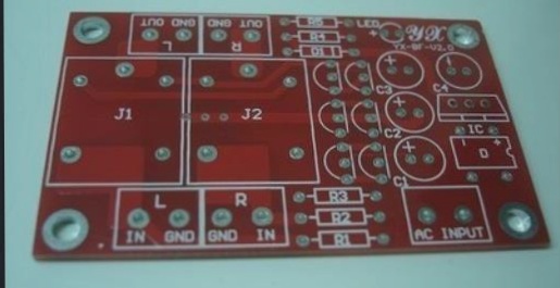
3. **Unreasonable PCB Circuit Design**
Designing a circuit with too thin traces while using thick copper foil can lead to excessive etching, resulting in copper loss or “dumping” of copper material.
2. **Laminate Manufacturing Process Issues**
Under normal conditions, as long as the high-temperature section of the laminate is hot-pressed for at least 30 minutes, the copper foil and prepreg will bond effectively. Therefore, the pressing process generally does not affect the bond strength between the copper foil and the substrate. However, during the lamination stacking process, if there is contamination of the prepreg or damage to the copper foil’s rough surface, it can result in insufficient bonding strength between the copper foil and the substrate. This may lead to misalignment (in the case of large panels) or sporadic copper trace lifting. Despite this, the peel strength of the copper foil near the lifted traces typically remains unaffected.
3. **Raw Material Issues in Laminate Production**
1. As noted earlier, ordinary electrolytic copper foils are typically products that have been either galvanized or copper-plated on a base material (known as wool). If the peak value of the wool foil is inconsistent during production or if there are issues during the galvanizing/copper plating process—such as poorly-formed plating crystals—this can reduce the peel strength of the copper foil itself. When poor-quality foil is used in PCB production, external impact during the assembly process can cause the copper traces to detach. In such cases, the copper rejection will not show obvious side corrosion when peeling off the copper trace, nor will the copper foil surface appear unusually rough. However, the overall peel strength of the copper foil will be significantly compromised.
2. **Poor Compatibility Between Copper Foil and Resin**: Some PCB laminates, particularly those with specialized properties such as HTG (High Tg) sheets, use unique resin systems. These resins typically employ curing agents like PN resin, which has a simpler molecular chain structure and lower cross-linking density. If the copper foil used in the laminate production does not match the resin system, the bond strength between the copper foil and the resin will be insufficient. This mismatch can result in poor peel strength and copper trace shedding during assembly when external forces are applied, such as during insertion into electronic devices.
If you have any PCB manufacturing needs, please do not hesitate to contact me.Contact me

