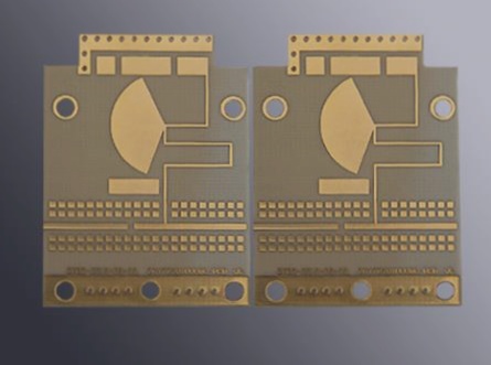
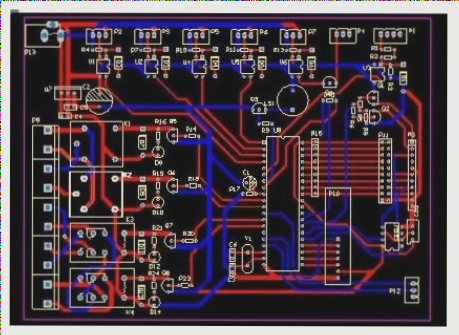
With the wide application of Digital Signal Processors (DSP), designing a high-speed signal processing PCB board based on DSP is crucial. In a DSP system, the operating frequency of the DSP microprocessor can reach hundreds of MHz. The reset line, interrupt line, control line, integrated circuit switch, high-precision A/D conversion circuit, and circuits with weak analog signals are susceptible to interference. Therefore, for a stable and reliable DSP system, anti-interference design is essential.
Interference, or interfering energy, can put the receiver in an undesired state. There are two types of interference: direct (coupling via conductors, common impedance, etc.) and indirect (coupling via crosstalk or radiation). Various electrical emission sources, such as light, motors, and fluorescent lamps, can cause interference. Electromagnetic interference (EMI) impacts through the interference source, propagation route, and interference receptor. Disrupting any of these factors can solve the electromagnetic interference problem.

Analysis of Interference Generation in DSP Systems
To ensure the stability and reliability of a DSP system, interference must be eliminated or minimized from all aspects. Interference in DSP systems mainly arises from the following sources:
1) Input and Output Channel Interference: Interference can enter the system through both the input and output channels. In the data acquisition link of a DSP system, interference can be superimposed on the signal through sensors, leading to errors in data acquisition. In the output link, interference can cause data errors or system crashes. Optocoupler devices can be used to reduce input and output channel interference. Electrical isolation can also be employed to address interference from sensors and the main DSP system.
2) Power System Interference: Interference from the power system is a significant source of disturbance in DSP systems. When the power supply provides power to the system, it may introduce noise. Therefore, decoupling the power lines during the design of the power chip circuit is crucial.
3) Space Radiation Coupling Interference: Radiation coupling, also known as crosstalk, occurs when electromagnetic fields induced by electrical currents in wires cause adjacent signals to distort or be erroneous. The strength of crosstalk depends on the device, wire geometry, and separation distance. In DSP wiring, increasing the distance between signal lines and proximity to the ground line can effectively reduce crosstalk.
Designing PCB Boards to Address Interference
In order to reduce interference in the fabrication process of PCB boards for DSP systems, the following methods can be employed:
Laminated Design of Multilayer Boards: Stacked designs of multi-layer boards are commonly used in high-speed digital circuits to enhance signal quality and reduce EMC. Dedicated power and ground planes should be allocated in a stacked design to suppress interference effectively. Components should be placed strategically to optimize routing space and minimize interference.
Layout Design: Careful layout of components is crucial in achieving optimal DSP system performance. Components such as DSP chips, Flash, SRAM, and CPLD devices should be placed thoughtfully, considering routing space and functional independence. Special attention should be given to high-speed signal layout, digital-analog device placement, clock layout, decoupling layout, power supply layout, and other component arrangements.
Wiring Design: Effective wiring techniques can further enhance the anti-interference capabilities of a DSP system. Properly routing signals, clocks, power, and grounding paths can significantly reduce electromagnetic interference. Techniques such as fan-out for BGA devices, clock signal routing, system power handling, grounding strategies, and other precautions should be implemented to mitigate interference.
By implementing these design considerations and techniques, PCB boards for DSP systems can be optimized to minimize interference and ensure the reliable operation of the system.
Interference, or interfering energy, can put the receiver in an undesired state. There are two types of interference: direct (coupling via conductors, common impedance, etc.) and indirect (coupling via crosstalk or radiation). Various electrical emission sources, such as light, motors, and fluorescent lamps, can cause interference. Electromagnetic interference (EMI) impacts through the interference source, propagation route, and interference receptor. Disrupting any of these factors can solve the electromagnetic interference problem.

Analysis of Interference Generation in DSP Systems
To ensure the stability and reliability of a DSP system, interference must be eliminated or minimized from all aspects. Interference in DSP systems mainly arises from the following sources:
1) Input and Output Channel Interference: Interference can enter the system through both the input and output channels. In the data acquisition link of a DSP system, interference can be superimposed on the signal through sensors, leading to errors in data acquisition. In the output link, interference can cause data errors or system crashes. Optocoupler devices can be used to reduce input and output channel interference. Electrical isolation can also be employed to address interference from sensors and the main DSP system.
2) Power System Interference: Interference from the power system is a significant source of disturbance in DSP systems. When the power supply provides power to the system, it may introduce noise. Therefore, decoupling the power lines during the design of the power chip circuit is crucial.
3) Space Radiation Coupling Interference: Radiation coupling, also known as crosstalk, occurs when electromagnetic fields induced by electrical currents in wires cause adjacent signals to distort or be erroneous. The strength of crosstalk depends on the device, wire geometry, and separation distance. In DSP wiring, increasing the distance between signal lines and proximity to the ground line can effectively reduce crosstalk.
Designing PCB Boards to Address Interference
In order to reduce interference in the fabrication process of PCB boards for DSP systems, the following methods can be employed:
Laminated Design of Multilayer Boards: Stacked designs of multi-layer boards are commonly used in high-speed digital circuits to enhance signal quality and reduce EMC. Dedicated power and ground planes should be allocated in a stacked design to suppress interference effectively. Components should be placed strategically to optimize routing space and minimize interference.
Layout Design: Careful layout of components is crucial in achieving optimal DSP system performance. Components such as DSP chips, Flash, SRAM, and CPLD devices should be placed thoughtfully, considering routing space and functional independence. Special attention should be given to high-speed signal layout, digital-analog device placement, clock layout, decoupling layout, power supply layout, and other component arrangements.
Wiring Design: Effective wiring techniques can further enhance the anti-interference capabilities of a DSP system. Properly routing signals, clocks, power, and grounding paths can significantly reduce electromagnetic interference. Techniques such as fan-out for BGA devices, clock signal routing, system power handling, grounding strategies, and other precautions should be implemented to mitigate interference.
By implementing these design considerations and techniques, PCB boards for DSP systems can be optimized to minimize interference and ensure the reliable operation of the system.


