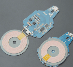
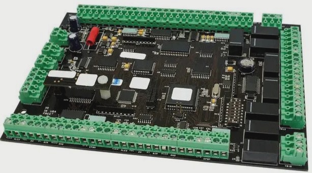
Electroplating is an essential process in the production of PCB boards. The coating of PCB boards varies according to their specific applications. Here is a brief description of the properties and uses of copper and nickel coatings from WellCircuits, a leading circuit board manufacturer.

1. Properties and uses of copper coating on PCB boards

The copper coating on PCB boards is rosy, soft, ductile, and easy to polish. It possesses excellent thermal conductivity and electrical conductivity. However, copper easily oxidizes in the air and quickly loses its luster, making it unsuitable as a surface layer for protective-decorative coatings.

Primarily, the copper coating on PCB boards serves as a foundational layer for multi-layer coatings involving steel and iron. It also frequently acts as an underlayer for tin, gold, and silver plating. Its primary function is to enhance the adhesion between the base metal and the subsequent surface or intermediate coatings, facilitating the deposition of these coatings. Utilizing thick copper and thin nickel plating processes in protective-decorative multi-layer plating can improve the corrosion resistance of surface coatings, thereby conserving precious nickel metal.

2. Properties and applications of nickel coating on PCB board

Nickel metal exhibits strong passivation capabilities, rapidly forming a very thin passivation film on part surfaces that resists atmospheric and certain acid corrosion. As a result, nickel coatings on PCB boards demonstrate exceptional stability in air. In nickel’s simple salt electrolyte, a fine crystalline coating can be achieved, boasting excellent polishing properties. Polished nickel-coated PCB boards retain a mirror-like gloss over extended atmospheric exposure. Furthermore, PCB nickel coatings possess elevated hardness and wear resistance. Based on these properties, nickel coatings are primarily utilized as base, intermediate, and surface layers for protective-decorative purposes, including nickel-chromium, nickel-copper-nickel-chromium, copper-nickel-chromium, and copper-PCB board nickel coatings.

However, due to nickel coatings’ high porosity, only thicknesses exceeding 25 μm can eliminate porosity, rendering nickel unsuitable as a general protective coating.

The production scale of nickel coatings on PCB boards is substantial, accounting for approximately 10% of global nickel production.

3. Copper plating process for PCB circuit board

Electroless copper plating, also known as PTH (Plated Through Hole), involves an autocatalytic oxidation-reduction reaction. Initially, active sites on the insulating base’s surface undergo treatment with an activator, typically utilizing palladium particles (though due to palladium’s high cost and volatility, practical colloidal copper processes are increasingly employed abroad). Copper ions are first reduced on these activated palladium particles, which then serve as catalytic nuclei enabling further copper reduction on their surfaces. Electroless copper plating is extensively employed in the PCB manufacturing sector, particularly for metallizing holes. The hole metallization process for PCBs is outlined as follows:

1. Drill hole

2. Deburr and clean the board

3. Rinse with ten washes

4. Chemical micro-etch for surface roughening

5. Rinse once

6. Pre-immersion treatment

7. Colloidal palladium activation

8. Rinse once

9. Accelerated gel removal treatment

10. Rinse twice

11. Copper immersion

12. Rinse ten times

13. Final rinse

14. Dry

Leave a Comment

Contact

WellCircuits
More than PCB

Upload your GerberFile(7z,rar,zip)